Because of the holidays, TI E2E™ design support forum responses will be delayed from Dec. 25 through Jan. 2. Thank you for your patience.

This thread has been locked.

If you have a related question, please click the "Ask a related question" button in the top right corner. The newly created question will be automatically linked to this question.

UCC27714: HB,HS,HO leakage failure

Guru 54778 points
Part Number: UCC27714
Other Parts Discussed in Thread: TIDA-00778

Three phase motor 12.5kHz PWM commutation 100VDC cause random failure to HS/HO junction, no signs of under/over shoot HO via soft turn on/off compensation resistors.

The means of using soft or even hard NFET turn on eventually damages HO Totem pole, stresses HS/HO internal NFET. Such results in leaking VDD supply onto 1/2 bridge inductor raising typical 12.6v floating bias to nearly 14.3v, e.g. HB leakage via HS/HO breakdown.

Conditions: 80us overlapping PWM drive signals HI/LI inputs, LO/HO:130 ohm GTon, 24 ohm GToff (parallel R/Schottky), NFET Qg=<96NC  @VBpin=13.6v

Contrast: Other vendor 600v gate driver (IGPK +/-600/350ma PW<10us) never fail similar described leakage, mandates unwarranted chip replacements.

1. How can maintaining IGPK +/-4amp (PW<10us) ever cause HO/HS stress via 130 ohm GTon 24 ohm GToff resistor?

2. What is work around to stop HS to HO reverse leakage path from developing in first place, typical HS pin R value?

3. Why does HO/HS leakage path failure cause uncontrolled and very high inductive voltage overshooting?  

4. Zener diode (15.2VzMin, 16.4VzMax @10ma) or 10k protection resistor placed across HS/HO, regulates floating VB the cause? 

5. Any Wiki report updates how to correct HO side gate drive failures caused from industry typical configurations?

  • Noticed the LO/HI GToff (24ohms) fall time seems a bit under compensated, ringing 1st pulse starts just above ground, tail ringing falls below too. Sorry don't see connection how Gtoff fall time could ever cause HO/HS leakage path to develop.

    The motor run time minimum pulse width is software regulated but the initial start up duty cycle sometimes <2us GTon rise times during the initial applied phase current. Initial startup duty cycle seems the likely place if any HO/HS could be stressed, though IGPK could never peak +/-4A with GToff = 24 ohms, correct?
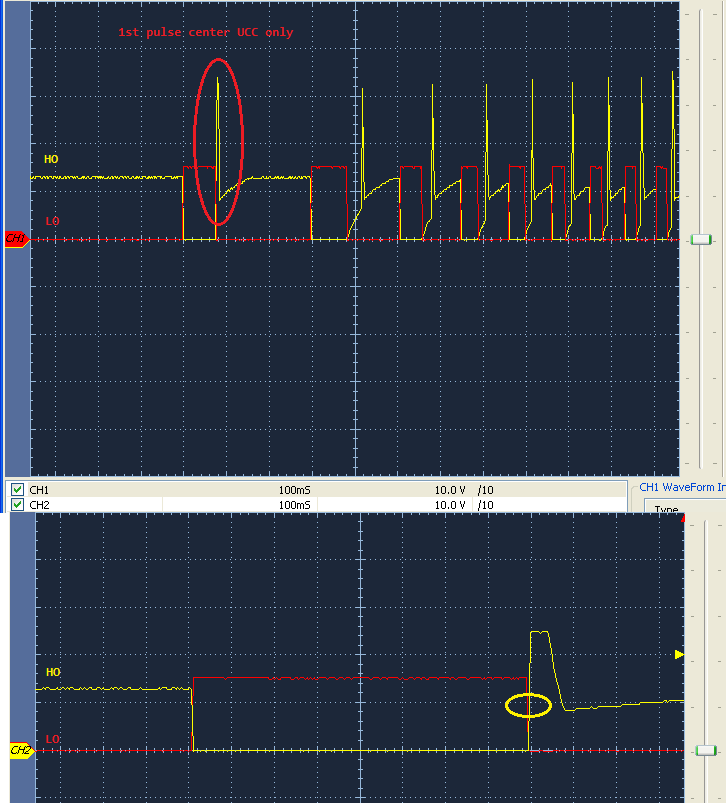
  • Center half bridge (NEW UCC) spiking HO on first NFET pulse (after precharge cycle) where other two UCC bridges do not have 1st overshoot pulse. All three 1/2 bridges VCC (+15v) and HO drive overshoots NFETs >36v peaks (without any inductors connected) @24VDS. How can >VDS pulses occur without any inductors connected on all three 1/2 bridges, is that behavior not troubling?
  • Hello BP101,
    From what you describe, is sounds like you are seeing the high side internal driver totem pole failure with the circuit you describe.
    I want to make sure there is not an external totem pole outside the driver, BJT follower for example, can you confirm.
    The other driver you mention is a 350mA source/ 600mA sink driver, please confirm if not correct.
    The competitor part that is rated at 600mA sink current may have been rated at a higher VDD/VHB voltage, 15V is common for some drivers.
    In this case, the UCC27714 with higher drive current may have higher sink current with the 24 Ohm turn off resistance, in your application at 13.6V VHB. This may result is some additional ringing on the Vgs.
    If there is suspected HO to HS negative voltage undershoot, we recommend a schottky diode from HO to HS placed very close to the IC pins to limit the negative voltage.
    On question 3, is there just an HO to HS higher leakage current failure in the application, or does the HO output stop generating output pulses. High leakage current on HB or HO will discharge the HB cap which can terminate the HO pulse due to UVLO before HI goes low.
    I would look at reducing the turn off resistance in the circuit, as the competitors driver may be lower current in you application VHB.
    If there is HO to HS negative ringing, I would suggest the HO to HS schottky diode to limit the negative ring, to see if these resolve the issues.

    Regards,
    Richard Herring
  • Hi Richard,

    Richard Herring said:
    The competitor part that is rated at 600mA sink current may have been rated at a higher VDD/VHB voltage

    VCC=25v absolute MAX, 20v recommended, VB=VS+20v. Does TI recommend +12 VDD over that of +15 VDD for <20 VGS NFETS?

    Richard Herring said:
    The other driver you mention is a 350mA source/ 600mA sink driver, please confirm if not correct

    GTon=120ohms, GToff=60 ohms same parallel Schottky with no (0) Qrr over shooting B+. This may be due to bipolar PWM switching as the Qrr ringing occurred mid supply, not top supply as it now does! That is the one major difference noticed between the competitions gate driver. Perhaps why we never saw any overshooting spikes into B+ and Schottky HS to AGND was to stop parasitic currents causing HI latch ups.

    Richard Herring said:
    In this case, the UCC27714 with higher drive current may have higher sink current with the 24 Ohm turn off resistance, in your application at 13.6V VHB. This may result is some additional ringing on the Vgs.

    There are no external Totem poles BJT's.  Values less then 24 ohms (GToff) short UCC HO/HS very quickly during open loop commutation cycles. Actually increased from 75 ohm up to 130 GTon has proven more prudent in protecting HO/HS stresses. Initially was stressing HO/HS on all three 1/2 bridges more frequently via 6-12ohm GToff thus created excessively high DS Tr overshooting on HV.  Also just removed 1uf caps Pin 5 AGND to VDD. Guessing 1uf to AGND perhaps injects delta winding Thriten harmonic PWM transients into VDD causing part of the (random) DS overshoot onto HVDC B+.

    Richard Herring said:
    If there is HO to HS negative ringing, I would suggest the HO to HS schottky diode to limit the negative ring, to see if these resolve the issues.

    The GToff undershoot ringing was minimal (<-4v) at 80-100vdc supply. Just replaced 24 ohm with 51ohm Gtoff and have not yet checked the difference. Checking LO/HO outputs the center (new UCC) at times HO crosses LO near 10v even with 60-80ns dead band.  Again why does first HO pulse occur yet does not on the other 1/2 bridges until after 2nd pulse and notice all HO pulses seem to occur mid Cboot charge rise time. That rising edge 1st pulse HO (CH2) during Cboot charge cycle seems to occur far to early does it not? At what level does HO/LO crossing cause shoot through? Suspect where HO/LO randomly cross 10v (yellow circle)  HO is actually just above LO. If shoot through is occurring might it explain HO/HS leakage path development but not blow fuses or short 80 amp NFETS?

    No inductors three bridges, center shown open loop commutated. Notice 1st pulse cycle rise time cut short and others start charging Cboot after PW occurs.

  • Richard Herring said:
    On question 3, is there just an HO to HS higher leakage current failure in the application, or does the HO output stop generating output pulses

    Being leakage was in the center phase it may have gone unnoticed until doing DMM to GND check but typically the resulting pulse is to much greater. Later check if UCC was causing fault trips during open loop commutation after HV transient suffered MCU VDD rail in the process. Leakage HV being the one attribute where 24v can multiply into over 90v peaks, with an inductor the NFET pulses peak well over B+.

    Leaky UCC: diode check HO-HS reads 1.29v drop, reverse leads 0.697v. 

  • Hi Richard,

    Richard Herring said:
    On question 3, is there just an HO to HS higher leakage current failure in the application, or does the HO output stop generating output pulses. High leakage current on HB or HO will discharge the HB cap which can terminate the HO pulse due to UVLO before HI goes low

    Zoom in on the HI HO signals all 3 UCC are similar short HO. Seemingly HI signal saturates Cboot with 50us pulse on HI, there is no UVLO in well filtered +15 VDD local bias 5.1R 10uf. One reason ? forum year ago why Cboot was calculated 1uf in TIDA-00778, formula in UCC datasheet suggest 122n/0.122uf Cboot.  Does zoom capture not appear as if Cboot has fully charged saturates near mid VDD, therefore stops pulsing? We don't see quite so much HO artifact as below capture during closed loop commutation as the trapezoidal wave form hides all but the recovery spikes shown above post capture.  

  • Hello BP101,

    In this post, and the previous post scope plots, to determine the driver operation I would need to see some more detail on the waveforms, as well as other signals.

    Also please confirm if the provided waveforms or with the UCC27714 driver that has the high leakage as you mention, or is not damaged yet.

    On the waveform in this post, It certainly looks like the HO is declining, I assume to HB discharging and going into UVLO. Is the CH1 waveform the HO with respect to ground, or is it differential with respect to HS?. Can you take this waveform again with one of two methods; Record HO, HS, HB, and HI; show wide time base as you have, and also zoom out to see more cycle information on the last few cycles before HO stops switching.

    On the plots shown in the previous post. It looks like this is HO with respect to ground, which is HO plus HS. Can you take those same plots showing the same HI, HO, HS and HB waveforms? I would like to confirm what HO is doing with respect to HI and HS.

    Regards,

    Richard Herring

  • HI Richard,

    Richard Herring said:
    On the plots shown in the previous post. It looks like this is HO with respect to ground, which is HO plus HS.

    Does it really matter where the threshold of HO is referenced if Cboot is being early discharged or saturated, take your pick. We only have two cannels to work with, captures are 1KSPS deep.

    Richard Herring said:
    On the waveform in this post, It certainly looks like the HO is declining, I assume to HB discharging and going into UVLO

    Countering that idea notice LO is not being effected by VDD droop as HO stops pulsing, abruptly overshoots VDD bias (14.7v) by 6v, peaks 36v, very early roll off relative to HI. Perhaps symptoms point to HB overcharge (saturation) more related would it not? We have also captured VDD bias during HB charge period remains very stable, if UVLO occurs it is not by external VDD circuit design. If Cboot (1uf) was being depleted at even QG 90NC what would HO look like relative to HI shown in capture? So the UVLO is auto resetting in each HO cycle during loaded inverter run time or simply reacting badly to an No inductive load condition? If the latter is occurring the current load of  any single phase is 0 every 240 degrees as only two phases commutate at any given time.

    Richard Herring said:
    Record HO, HS, HB, and HI; show wide time base as you have, and also zoom out to see more cycle information on the last few cycles before HO stops switching.

    Why not simply reduce Cboot 100n or even 50n record what happens? The HO drop occurs early on all three gate drivers makes it unlikely UVLO is occurring from driving an unloaded NFET, does it not? Also noted inverter run time tight ringing pattern at Miller plateau, seems to indicate Cboot being suspect, seemingly not UVLO. If UVLO was occurring it would effect the ability for motor to even run under heavy load, correct?

  • Hi Richard,

    Richard Herring said:
    I would like to confirm what HO is doing with respect to HI and HS.

    Ok we try different approach change Cboot 100n thus discover HI input RC filter somehow changes PWM generators PW=2.5us versus 50us, relative 1uf Cboot captures above. Does the UCC charge pump really need to exceed VDD even overshoot it each and every HO pulse? Notice with 100n Cboot first few pulses only overshoot VDD then drop down to VDD relative to GND.  Oddly the other 2 UCC (1uf Cboot) only reach VDD (14.7) bias on the first pulse, next pulses overshoot VDD >19.7v, a 5v net increase over VDD bias 10uf cap.

    Checking the competitions gate driver (Cboot 1uf) HO produces similar VDD overshoot 50us pulses but does not cause excessive B+ overshoot in the NFETS as UCC last capture. That seems the primary issue to why the UCC H0-HS junction can quickly break down start leaking and Cboot cap value HO issue seems related to the Trr overshooting.

    NFET Trr ringing overshoots B+ 80v not any less at 100v:


  • The confusing issue being Cboot 1000n limits HB-HS PW to 50us, 50% duty, no matter HI start pulses < 2.5us. Note the HO drive PW starts (2.5us) transitions into 20us PW. Yet the high HS peaks >36v first pulse, thereafter with 100n Cboot are missing in 80us PW (300ms HO period) CH2.

    Seemingly no voltage regulation of HB exists to compensate for Miller PCHAN boost modification. Therefore Cboot bias (14.7v) can exceed VDD max thus cause HOPW peak concerns! There was plenty of energy (Cboot 100n) to wield 36 pound rotor in open loop commutation. However the huge EMF/EMI 1000n Cboot caused now diminished requires lower db FOC adjustments. Perhaps TIDA-00778 should reevaluate as we have the ill effects of 1000n Cboot choice, OGBT module might run more efficiently if not being over driven.

  • Hi Richard,

    The captures are from replaced UCC, the leaky HS-HO was bad & removed. The issue most intriguing initial HI into HO output PW was over ridden by Cboot RC rule over HI PW. Notice I changed 50us to 20us PW above after checking it again this AM, 100n Cboot reduced the initial open loop PW <10us may have previously caused odd stressing?

    There is minor mV HO ring though not close to the amplitude shown in last capture. Remains a mystery why HV overshoot is so much greater than mV HO ringing, so small must zoom out to verify tiny mV peaks even @10KSPS deep. The NFET B+ overshoot remains an issue even with NFET 20-40% faster Qrr via Infineon fast diode technology, run 10*C cooler. By HO overshoot would not that be several hundred millivolts or more to consider minor peak ringing an overshoot condition?
  • The replaced UCC was immediately stressed (HO-HS) simply from setting PWM frequency from 12.5kHz to 40kHz with 80VDC supply. Hard to imagine even a marginal NFET gate region causing such immediate stresses to HS given 130 ohms GTon, 51 ohms GToff. Obviously datasheet claims (guaranteed by design) IGPK +/-4A <10us PW is not holding true via CUT, even with Cboot 100n produces initial HO PW <2.5us.

    Note 24vdc supply setting 40kHz seems to cause no stress to HO-HS driver causing greater HS damage at 80vdc than 24vdc. Oddly the LO/HO drive Gton up to 90% takes roughly 2.5us very slow rise partially caused 200pf/51ohm filter on HI/LI inputs.