This thread has been locked.

If you have a related question, please click the "Ask a related question" button in the top right corner. The newly created question will be automatically linked to this question.

LMR23625: Radiated emissions issue

Part Number: LMR23625
Other Parts Discussed in Thread: LMR33630

Dear all,

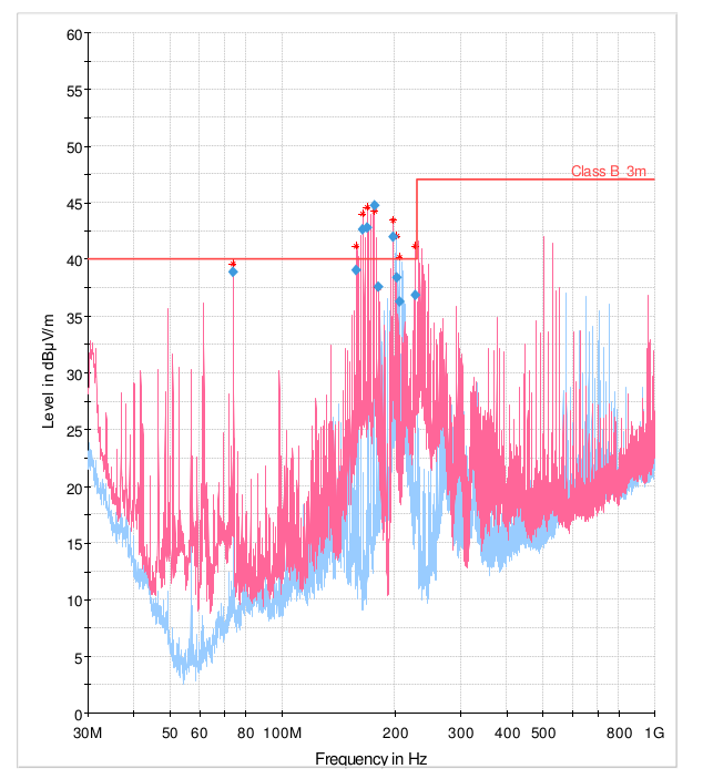
we are having problems passing EMI certification with a product using LMR23625 buck converter (12V to 5V). Specifically, we are failing the radiated emission test in the 35-40 MHz and 150-200 MHz regions (depending on the configuration of attached cabling during test). We suspect that the issue is with this buck converter since the frequencies of problematic emissions are multiples of 2.1 MHz LMR23625 switching frequency and appear also when other parts of the device are removed or powered off.

We attempted to reduce the dV/dt of the switching node by placing a 33 ohm resistor in series with BOOT (C10) with no apparent effect. Approx. 10 mV peak-to-peak ringing in the 35-40 MHz region is clearly visible on the oscilloscope on 12VIN, however the switch node waveform seems clean, with no overshoot or ringing (but that might the effect of scope probe). Based on the literature available from TI we suspect that the issue is with the PCB layout, but after 3 PCB iterations we failed to find the exact cause. The issue disappears if we use a 4-layer board with 2 inner layers having only ground fills, however if possible we would like to use a 2-layer board in this application.

Thank you for any help and best regards,

Tomaž

  • Tomaz,

    I sympathize with the EMI struggle. The layout looks pretty good. Here are some suggestions which should help the EMI results:

    Quick test board modifications:
    1. Make sure the inductor L1 is soldered with the dot facing the SW node (your L doesn't appear to have a dot. Just try rotating it 180 degrees). The dot denotes where the winding starts (center of the coil) so the quieter VOUT side of the inductor will be on the outside of the coil. Free shielding from capacitive coupling and it can make a big difference.
    2. Scrape off some solder mask and place a 100nF 0603 ceramic cap above L1, next to C9, connecting VOUT to PGND. This will redirect the high-frequency content in a smaller loop.
    3. Try a different filter inductor (L2). Smaller parasitic capacitance should help.

    Layout changes:
    1. Reduce the size of the SW node. Make it only wide enough to pass the current, no wider.
    2. Move the boot cap as close as possible to the SW and BOOT pins
    3. Place a 100nF ceramic cap just above the inductor, next to C9 connecting VOUT to PGND. This redirects high-frequency content back in a smaller loop (same as #2 in quick test board modifications).
    4. The VIN trace from the filter to VIN at the IC is long with no GND plane underneath. This means the return path will form a larger loop which allows for more coupling from other loops in the system.
    4. Worst case, add a common-mode choke. That will help immensely but it may be cost prohibitive.

    Bigger changes:
    1. I'm sure we can get this board to pass with this part but you might consider a part which will make EMI easier. LMR33630 for example is in a hotrod package. No bond wires and intuitive pinout means great EMI.

    -Sam
  • Dear Sam,

    thank you for a very comprehensive answer! As far as I can measure with an oscilloscope, L1 orientation and 100nF on VOUT don't appear to make any significant difference on 12VIN noise in the 40 MHz region. I can't really measure radiated emissions in our lab. I also tried 3 different filter inductors. We'll need to do another run at the certification lab to try it out.

    I think your suggestion about a ground plane under VIN is most promising. I looked back at a similar older design that did pass certification and that one did indeed have a more direct return path directly underneath VIN. I'll try to add one to this layout as well.

    Thanks again. I'll report back when I have more conclusive results.

    Best regards
    Tomaž
  • Tomaz,

    L1 orientation changes the amount of common-mode noise (capacitive coupling). This will make an extremely small change as seen on an oscilloscope but will greatly help EMI. EMI (especially radiated) are especially sensitive to common-mode noise since the power lines from source to DUT are close and in parallel. Common-mode noise creates constructive interference which radiates a lot.

    I look forward to hearing from you again.

    Threads on E2E lock after 30 days from the first post so I'm going to close this thread. Please post a new thread once you have results and refer us back to this thread. Thanks!

    -Sam