This thread has been locked.

If you have a related question, please click the "Ask a related question" button in the top right corner. The newly created question will be automatically linked to this question.

LM5030: PWM outputs not working

Part Number: LM5030
Other Parts Discussed in Thread: LM3411

Hi,

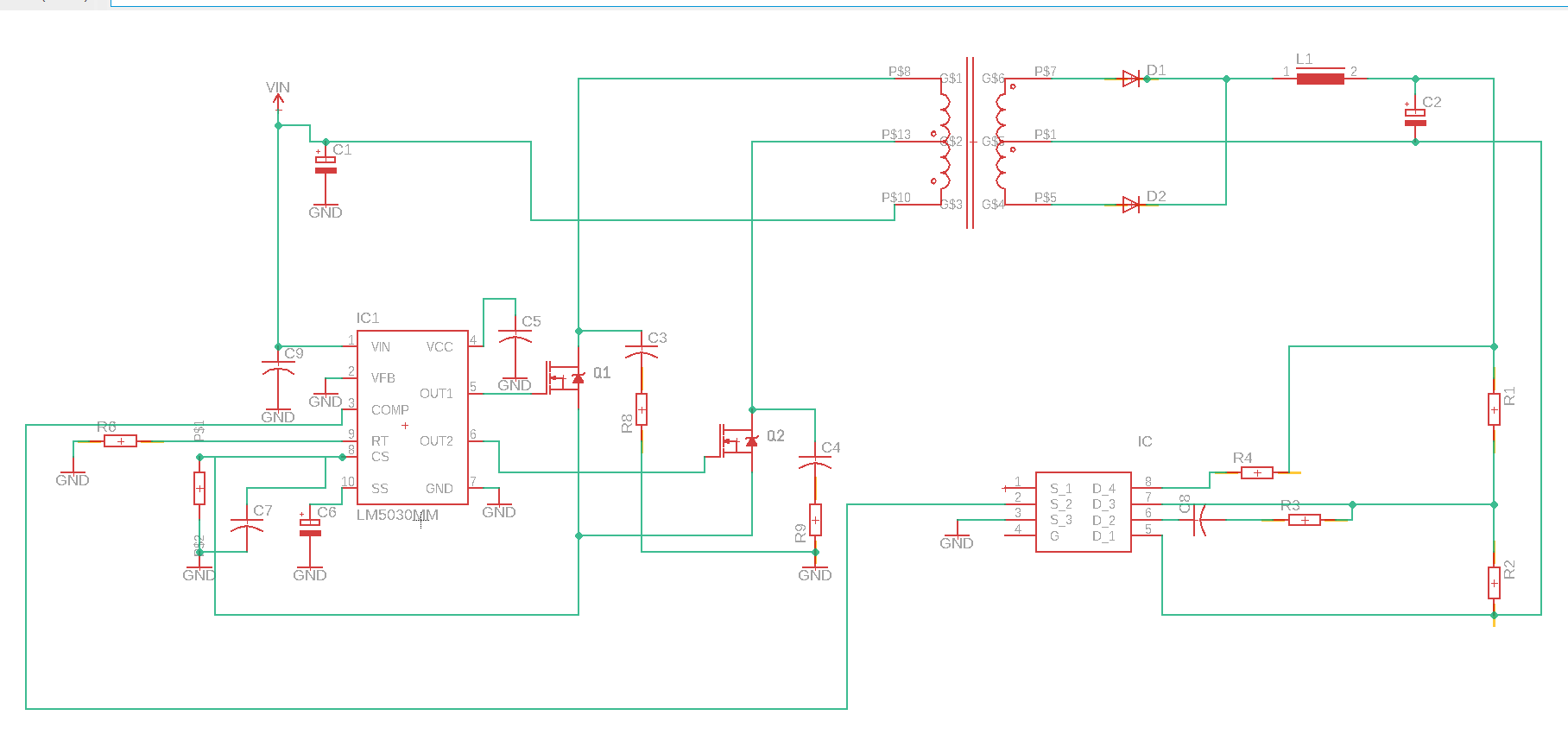
This is my first time here. I hope my problem gets resolved. I am designing a push-pull converter using the LM5030 IC. I have tried the implementation on my PCB but the two outputs are not giving out voltages. I initially thought that the IC got damaged due to heat from solder reflow, but I have soldered over 5 ICs on PCBs yet none of them gives any waveform on the outputs. I measured the following voltages.  Vin = 17.4V, Vfb = 0, COMP = 0.8v, VCC = 7.8V, SS = 4.92V, Rt = 2.04V, CS = 0V, OUT 1 =0, OUT 2 = 0. I have checked for short circuits but there is none. My latest suspect is the capacitor values. My question is do the capacitor values of VCC and SS decide if the output works. Otherwise, what could possibly be wrong with my measured values. 

Thanks

Austin

  • Hi Amalachukwu Okeke,
    Welcome to E2E.
    I am not able to give a complete answer without your schematic. Fortunately I can give some pointers based upon the details that you have provided.
    Having no outputs is likely due to the low COMP pin voltage. Please refer to the Block diagram given in Section 7.2 of the datasheet. You will notice that if the COMP pin voltage is 0.8V then the voltage on the '-' input of the PWM comparator will be at or below GND. In other words the TON period will be terminated immediately. Hence the outputs will be high for zero time.
    The next question that we must ask is why is the COMP pin voltage low when Vfb = 0. Normally if Vfb is pulled low the COMP pin voltage should be high (5V). Hence I need to know what you have connected to the Vfb and COMP pins that may cause this unexpected operation.
    I hope these comments assist you.
    Thanks
    Joe Leisten
  • The above is the schematic. The second IC is an optocoupler ( FOD2712AR2) the COMP pin is connected to pin 2 of the opto coupler which is the collector of the phototransistor. On the PCB, the Vfb pin is directly connected to the GND pin (pin 7). I am just confused as to why the COMP pin isn't going to 5v despite Vfb being 0 ( 0.05V as measured with an oscilloscope, same voltage with GND). Note that other components of the push-pull converter have been connected. On the second IC which I soldered to compare performance. The values are same as above, but the SS =0.8V and the COMP = 1.34V (on this PCB, I have not connected other parts of the converter, just the timing resistor and capacitor for VCC and VIN)

  • Hi Amalachukwu Okeke,
    This part of the schematic looks fine and the COMP pin voltage should be around 5V.
    May I suggest that you try disconnecting the opto-coupler from the COMP pin. It may be that the opto-coupler circuit is damaged and is pulling down the COMP pin.
    May I also suggest that you add a 1k resistor between your current sense resistor and the CS pin. This should help to protect the controller in the case of poor layout. Could you please advise the value of resistor that you currently have connected between the CS pin and GND (we normally call this the CS or current sense resistor).
    I did happen to notice it looks like the primary of your transformer is not connected correctly for a push-pull configuration. The input voltage should connect to the center tap of the primary and the two MOSFETS should connect to the upper and lower taps.
    I hope this helps
    Joe Leisten
  • I will disconnect the optocoupler as suggested. Meanwhile, the transformer connection on the PCB is different from what you see on the schematic, this is due to the way I wound the transformer (the Vin is on the centre tap). My current sense resistor is 25 milli-ohm. (for maximum primary current of about 19A
  • I disconnected the optocouupler and got an output voltage of 127V, expected is 120V. I connected a new optocoupler and the output voltage dropped to 38V. I guess this is now an optocoupler issue. I will work on it. Thanks a lot, I appreciate
  • Hi, do you have any idea why the MOSFETs could get hot even without any load at the output. Judging by the schematic I sent.

    Thanks
  • Hi Amalachukwu Okeke,
    Sorry for the delayed response. Your additional question got lost because the post was marked as resolved.
    Could you please give me some idea how much input power is flowing when the output power is zero?
    This should help to give some idea of the magnitude of the issue.
    Thanks
    Joe Leisten
  • The input current is about 0.2A while the input voltage is about 15v. However, when a load is connected, these input values remain unchanged, and the output voltage immediately drops from over 120volts to about 11volts

  • Hi Amalachukwu Okeke,
    It would be great if you could send some waveforms showing both of these operating cases (loaded and unloaded).
    The best waveforms to show would be:
    1) OUT1 voltage
    2) CS pin voltage
    3) COMP pin voltage
    4) Drain voltage of Q1
    Our office is on holiday until 3rd Jan so there will be a short delay. If this is a problem for you please post a new question which will be answered by one of our other offices.
    Thanks
    Joe Leisten
  • Hi Joe, the attached file contains the requested waveforms. I am also thinking if an undersized filter inductor and capacitor could cause that. The output voltage drops from 120V to about 10V when a load is connected, even the smallest of loads. I use FOD2712AR2 chip for feedback, which is an optoisolator and voltage reference combined.

    waveforms.pdf

  • Hi Amalachukwu Okeke,
    Thanks for the waveforms.
    It is clear from them that there is something very wrong with the power stage.
    I know this because the ON periods of the two switches should be equal.
    If you imagine the transformer to be ideal then regardless of which switch is ON the same voltage (VIN/N) should be applied at the left of the output inductor. This should cause the inductor current to ramp up.
    The inductor current /N should be detected as a voltage across the current sense resistor and the ON period of the pulse should be terminated when the inductor current reaches the required level. This process should be the same for both switches giving the same ON time. You are showing very short ON periods for OUT2 and long ON periods for OUT1.
    If the actual ON periods applied to the transformer are like this then the transformer must saturate.
    Please check your power stage very carefully. Look for things like:
    1) One of the transistors Q1 or Q2 is not being turned ON or is damaged.
    2) Transformer phasing is not correct. When each transistor is turned ON it should give a positive voltage at the left of the output inductor.
    3) On of your output diodes is damaged
    You will know when the circuit is working properly because the ON periods of both outputs should be approximately equal.
    Hope this helps.
    Joe Leisten
  • Hi Joe,

    Thank you for this elaborate explanation. I noticed the problem of the different ON times of the two switches, it is actually a new development as they were equal when I first implemented the circuit, and the output voltage still dropped to 10V when loaded. Although, I noticed that my output diodes were undersized. I have decided to design a new transformer, get different MOSFETs and diodes and also change the optocoupler chip which has both the optocoupler and voltage reference in same chip to a more conventional (LM3411 voltage reference and an optocoupler). I hope this would solve my problem. I would revert on the outcome when completed. Thanks again for your time, I appreciate.

  • Hi Amalachukwu Okeke,
    I will mark this thread as closed/resolved. Please feel free to open another if you have any further questions.
    Joe Leisten