This thread has been locked.

If you have a related question, please click the "Ask a related question" button in the top right corner. The newly created question will be automatically linked to this question.

TPS53353: 0Ω condition for Boot capacitor

Guru 19645 points
Part Number: TPS53353

TPS53353 datasheet is described that Boot capacitor(R9) recommend is 2Ω.

①If noise and ringing condition is good, is Boot capacitor set to 0Ω, no problem? 

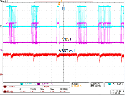
※One customer waveform is attached below, large Boot cap will be drop VBST(with respect to LL).

 When change to less than 2.4Ω, VBST voltage was not drop.

 Customer want to confirm OK or NG for 0Ω condition. (When NG, what is the minimum value?)

・22Ω

・5.6Ω

・2.4Ω

・0Ω

②Additional question, datasheet P27 is described "Use separated vias or trace to connect LL node to snubber, boot strap capacitor and ripple injection resistor. Do not combine these connections."

 When combine snubber and ripple injection resistor, is there possibility for above VBST voltage drop?

 Please let me know about how influence the combine these circuit.  

Best regards,

Satoshi

  • Hi Satoshi-san,
    If noise and ringing condition is good, is boot resistor set to 0Ω, no problem? Yes.
    The VBST drop during the initial turn-on of the HS FET is normal. However, the HS FET has the turn-on threshold voltage of around 1.5V to 2V, so to be on the safe side, I would keep the drop above 2.5V. Please keep in mind that higher Rboot will effect the efficiency as well. You can also use the snubber circuit to minimize the switch node ringing to stay within your specification.
    As for combining the circuit on page 27, I believe the effectiveness of each circuit role would not be optimized if you combined the LL node together with one via.
    Thank you.
    Amnat