This thread has been locked.

If you have a related question, please click the "Ask a related question" button in the top right corner. The newly created question will be automatically linked to this question.

TINA/Spice/LM5085: Current Limiting function; Is it implemented in the transient model?

Part Number: LM5085
Other Parts Discussed in Thread: TINA-TI, , LM25085

Tool/software: TINA-TI or Spice Models

Hi, I have been taking a look at the LM5085 for use in a simple battery charger role. One of the things that atrracted me to the LM5085 is the fact that it can operate with 100% duty cycle. This was important as the design is primarily that of a current limiter. Vin = 60V and this is a stable source coming from a another SMPS. This power supply is feeding the main system but I also wish to use it as a power source for a battery charger. However I must ensure that when the main system is pulling high current the battery charger (LM5085) is able to reduce the current it delivers to ensure that the SMPS is not overloaded.

So under light system load the LM5085 should pass high currents up to ~ 8A @ 60V(Vout). i.e 100% duty cycle with only the Rds_on drop seen between Vin > Vout. Under heavy system load, the LM5085 must be re-programmed to reduce the maximum current. Exactly how this might be achieved is still to be decided.

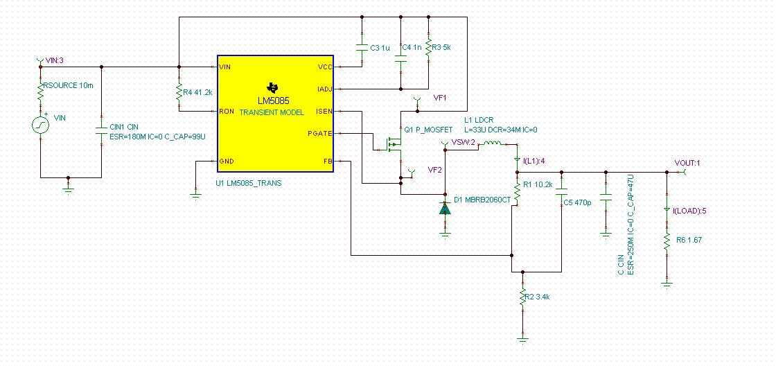
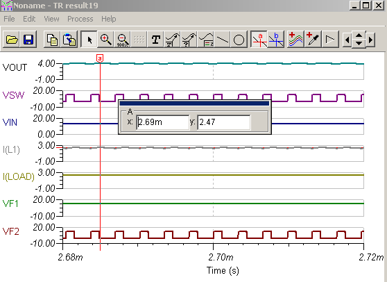
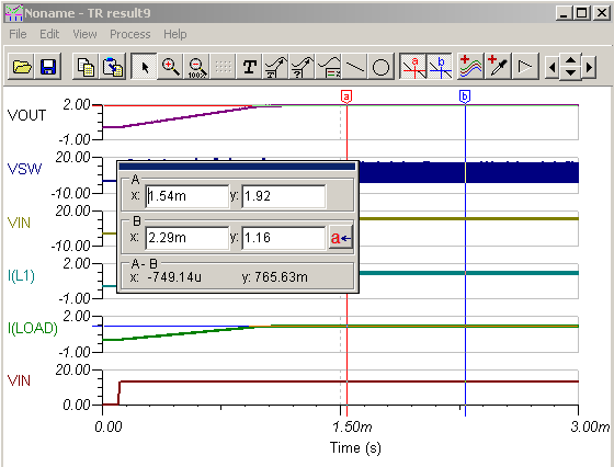
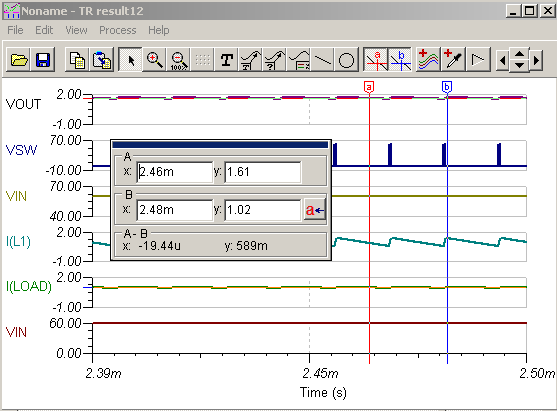
However my question is around the LM5085 transient model in TINA. I can not seem to get the current limiting function to act as expected. I have tried lowering the regulated output voltage to well below the level of Vin, but even under this configuration the model does not seem to trigger any off-time for the gate when ADJ is above ISEN. Even if I force the ADJ pin to a higher voltage than the ISEN pin, it seems to make no difference to the PGATE output. 

So could you confirm that the model actually has implemented the current limit function. If you believe it is implemented could you suggest a configuration or better still share with me a simple TINA file that demonstrates the current limiting working. 

All the best

Aidan

  • Aidan,

    Let me check with the modeling expert and get back to you. You can expect a response in the next day or so.

    -Sam
  • Thanks Sam,
    FYI, I also today looked at the Application Report AN2157 "Constant Current Constant Voltage Buck Converter With LM25085 , or , Implementing Accurate Current Limit With LM25085"

    I implemented the circuit of Fig2 exactly as seen in the App Note within TINA. The aux circuit does exactly what is expected and the ISEN pin is indeed pulled down when the current exceed 2.5A as described, but the LM5085 model does not react.

    However if I replace the LM5085 transient model with the LM25085 pspice transient model imported into TINA, then the circuit current limits as expected.

    This gives me confidence to report that I'm now quite sure your LM5085 TINA model does not work with regard to current limiting.
    Aidan
  • Hi Aidan,

    We are looking into it.

    Best Regards,
    Ashis
  • Hi Aidan,

    We have  looked into it and found that the device has current limit implemented in it.

    As per the Datasheet the current limit equation is given by :

       where RADJ=5k ,RDSON=87.547

       Giving ICL=2.284A .

    and the simulation results gives ICL=2.47A though we are demanding a load current of 3A .Please note that as the current limit is hitting at  2.47A,VOUT regulating around 4V instead of regulation target of 5V. Below are the snapshots of test set up and simulation results.

    Please also see the attached .TSC file of the test setup.

    LM5085_Current_limit.TSC

    Best Regards,

    Ashis

  • Hi Ashis,

    Thanks for your reply. So yes, I agree that your simulation does seem to exhibit current limiting. However I ask you respectfully to take a closer look at what is going on. For example, take a look at your simulation file and see what happens if you raise the input voltage from 13 to 15V ( No other change just raise the piece wise step of the voltage source to 15V). This is a very small increase in supply voltage but the effect is dramatic. You will see that this change alone stops the current limiting from working completely. 

    Now if I assume some FET characteristics like those in your datasheet for the LM5085 (td = 57nS + 50nS), we can calculate from the values of Rt used in the design that the expected operating frequency should be around 590KHz. Even if we raise the input voltage as described the effect of a recalculated Rt would brings its value from 41.2K down to 41K. This is a very small change, but if we adjust this value the current limit still does not work.

    Still further if we leave the new value for Rt at 41K but again drop the supply voltage to 13V, current limiting starts working again. 

    And further still. If instead of supplying the voltage at ISEN from the FET (or a sense resistor) but instead use a simple potential divider between Vin and GND, to ensure that we can set the ISEN pin at a much lower voltage than the ADJ pin, we should see that current limiting is always active. Doing this with a 13V supply does indeed act as expected and the output current is held off almost totally at approx 200mA.

    Now again with this potential divider configuration if we raise the supply voltage to just 15V, current limiting stops working completely. In fact raising Vin to just 14.5V stops it working and after some repeated tests like this, you will see that between 14 - 14.5V the current limiting starts to rise up somewhat exponentially until at about 14.5V+ it becomes almost totally ineffective. 

    You may ask why would I wish to use such a configuration, but in fact this is very similar to what you are suggesting in the application note that I referenced earlier. Whereby the ISEN pin is pulled low via a 431A precision shunt regulator. My own design uses a similar configuration as my current monitoring circuit is fed from another circuit altogether and not local to the LM5085. However I digress.

    I find it hard to believe that this behaviour is expected. After all this would be quite sensitive; a circuit where current limiting suddenly stops working if the supply voltage unexpectedly wanders a little above the design parameters.

    Perhaps I have not fully understood the operation of the limiter, but from the functional diagram it seems it is a simple comparator. If after the initial blanking period the ISEN pin is at a lower voltage than the ADJ pin, the FET should be held off. No mention is made as to any further complexity, or timing, or relative voltage differences between ADJ and ISEN and to further add to the confusion, as I said the LM25085 simulation does work just as expected, regardless of the supply voltage.

    This cant be right, can you please take a better look, or give me a much clearer explanation as to the exact functioning of the circuit. I am now starting to ask myself which model do I trust? Which is correct?

    And finally as a still further element of confusion. The LM25085 model seems to work as expected, like I said, BUT, if I connect ISEN to the DRAIN of the PFET, it does not seem to work. The circuit simply wont start. It seems that connecting the ISEN pin to the drain, stops the simulation from even attempting to switch the FET, very odd.

    All in all, I'm left confused, no knowing which simulation is correct, or which model I should trust to be an accurate representation of the component. Hmmm... please help.

    All the best

    Aidan

  • Hi Ashis,

    I have done a little further investigation and found the following. By taking a look at the un-encrypted spice model of the LM5085 I find the following line:

    E_ABM100         ISEN_1 0 VALUE { if(V(PGATE)<((V(VIN)/2)-0.5),V(ISEN),(V(VIN)+0.5))}

    I don't understand exactly why this line exists but it is the cause of the problem I am seeing. After initial startup, the voltage of PGATE will only ever fall 7.7V below VIN, this is dictated by the VCC regulator used to supply the bias voltage for the PFET. Nothing in the schematic block diagram suggests that this is a part of the circuit, but surely I cant know what is actually inside the IC!

    But this line compares the PGATE voltage to VIN/2 - 0.5. So if the voltage on VIN > ~14.4V then the ISEN value is always ignored. This seems to be supported by the tests I refereed to in my last post. 

    Indeed if the line in the SPICE file is adjusted as follows:

    E_ABM100         ISEN_1 0 VALUE { V(ISEN)}

    Then current limiting works again with higher input voltages, BUT stops working for cases where Rds_on is used as the sense technique. So I assume this line in the spice file is related in some way to the Rds method.

    I have looked further into the subckt but it is not so simple to work out what is going on. So before I go any further, and perhaps work around something, but end up with an unrealistic model. Perhaps you can explain what is going on here. 

    Looking at the revision history of the file, it is clear that this Rsen ... Rds_on current limit was added as a revision. I don't wish to assume anything much, but is it really working as expected.

    Aidan

  • Hi Aidan,

    We are working on it. We will keep you posted about the updates.

    Thanks,

    Somen

  • Just checking in for any updates. I am having similar problems with the LM5085/LM25085 spice models. The LM5085 posted above does not work at higher voltages, and I can't seem to get the sense-resistor based current limit to function at all for the LM25085 even at reduced input voltages.
  • Hi Aidan,

    We are looking deeper into it.We have modified the  "E_ABM100         ISEN_1 0 VALUE"  equation  but with this current limit is hitting for lower current as well.

    We also tried to simulate the test set up replacing PMOS with a switch and faced convergence issue.We will keep on updating on this. 

     Best Regards,

    Ashis

  • Hi Aidan,

    We are still debugging the model and following are the findings :

    1.We modified "E_ABM100 ISEN_1 0 VALUE" equation to add dependencies on GATE driver instead of VIN and validated current limit test across the entire VIN(5.5V-60V)range but still Current limit was not working .Then we found that the PFET RDS(ON) is varying as a consequence of that the device was limiting current at a lower value than the expected one.

    2.We replaced PFET by a switch and validated current limit test again for the entire VIN(5.5V-60V)range .Current limit is working fine up to a VIN range of (5.5V-45V) beyond which current is getting limited but the switching is not proper.

    We are working on it and will keep on updating on it.

    Best Regards,

    Ashis
  • Hi Aidan,

    We have modified the netlist to debug the issue and tested the below cases :

    1.VIN=13V,ILOAD=3A(with RDSON/RSEN)

    2.VIN=13V,ILOAD=0.5A(with RDSON/RSEN)

    3.VIN=5.5V,ILOAD=3A(with RDSON)

    4.VIN=5.5V,ILOAD=3A(with RSEN)

    5.VIN=60V,ILOAD=3A(with RDSON)

    6.VIN=60V,ILOAD=3A(with RSEN)

    The model is working fine and the results are coming as expected.

    Following are the simulation results of few cases mentioned above:

    Simulation results for VIN=13V,ILOAD=3A (with RDSON):

    Simulation results for VIN=13V,ILOAD=0.5A (with RDSON):

    Simulation results for VIN=60V,ILOAD=3A(with RDSON)

    Simulation results for VIN=60V,ILOAD=3A(with RSEN)

    Please let us know if you want us to test any other test cases otherwise we will release the model with fix as well as GATE Drive current issue fix posted by you in another E2E forum request by the end of this month.

    Best Regards,

    Ashis

  • Thanks Ashis,
    Looks good. I'm keen to test my own design and hopefully remove the gate buffer, should the model prove to be successful. I have to say, I find it hard to believe that the relatively low gate capacitance of the FETs I'm using would not be quite easily switched by the IC directly. However I will still need to be careful to model this from a thermal perspective. Its a trade of ... if I don't switch the FET hard, it will get very hot. If I switch the FET hard then the gate driver will get hot. So, I really would like to get as accurate a view as possible, then I know what the best approach will be.
    Something tells me, I might actually be better to leave the buffer in place. I have a better chance of cooling the gate drive, if its using discrete transistors.

    Anyway, end of the month is almost upon us. Have you posted the updated model yet?
    All the best
    Aidan
  • Hi Aidan,

    Initially we thought of releasing the updated model by end of the month. Considering our current bandwidth, we might not be able to release the model by this month. But we will try to release the model as soon as possible. For now we are not committing any date but we will inform you once the model is released to web.

    For now we are closing the thread. Sorry for any inconvenience.

    Thanks & Regards,
    Arpan Gupta