


Hi,
Could you please help to check the schematic below? Thank you.
1. The COM should be connected to the VSS directly or connect to the GND of Low side MOSFET?
2. Please help to that is their needs to be modified.
Thank you,
C.T.
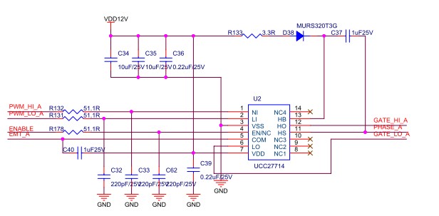
Hi,
Could you please help to check the schematic below? Thank you.
1. The COM should be connected to the VSS directly or connect to the GND of Low side MOSFET?
2. Please help to that is their needs to be modified.
Thank you,
C.T.

