Hi there,
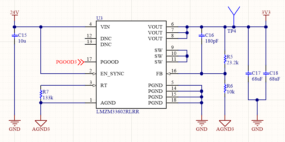
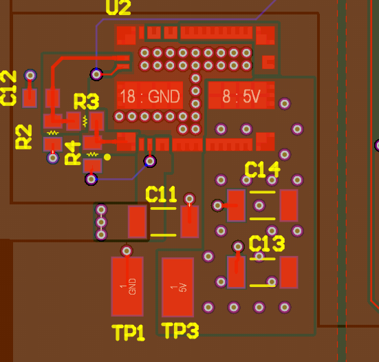
I have created a PCB using the LMZM33602 but I can't get it to output the 5V and I was hoping someone could look over my schematic/pcb do see if they notice anything odd. I am attaching both documents. Thank you! 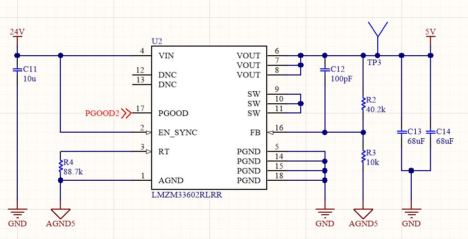
Hi there,
I have created a PCB using the LMZM33602 but I can't get it to output the 5V and I was hoping someone could look over my schematic/pcb do see if they notice anything odd. I am attaching both documents. Thank you!