This thread has been locked.

If you have a related question, please click the "Ask a related question" button in the top right corner. The newly created question will be automatically linked to this question.

TPS63020: TPS63020 question and design review

Part Number: TPS63020

Hi TI member,


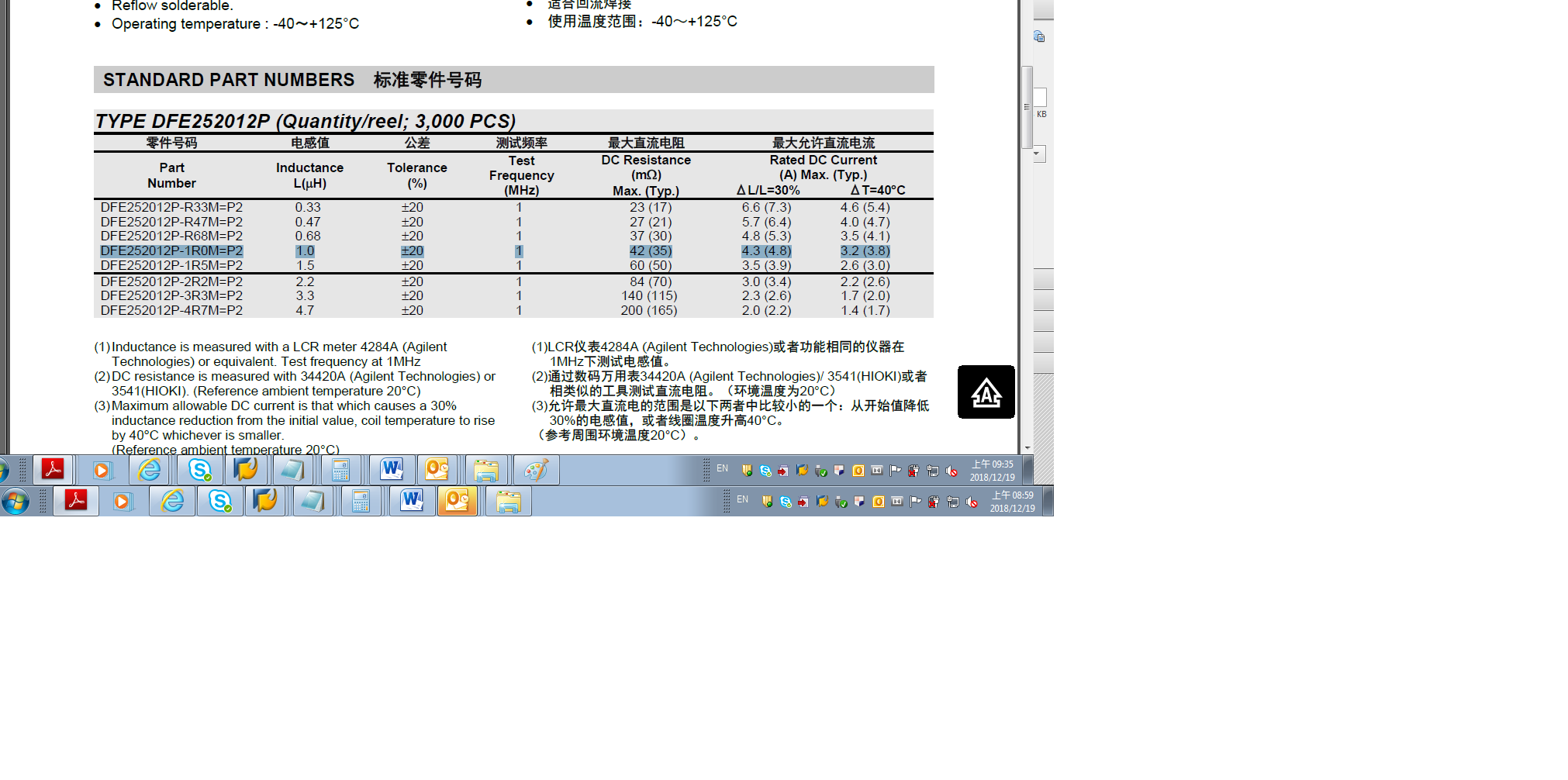
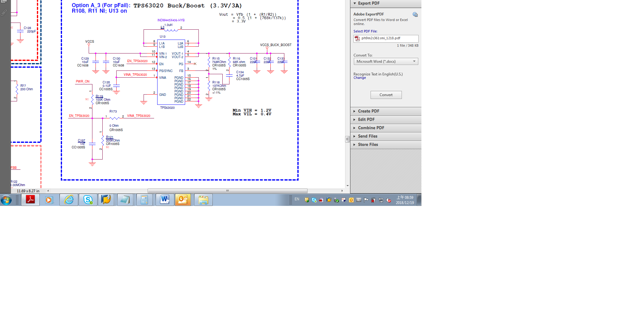
We are using your TPS63020.

Can we use it under the conditions below?


Input power: 3.45V~2.6V; But the normal condition will keep the input at 3.3V.

Output power: 3.3V

Output Current: 2A


If you cannot accept the gap between input power and output power is 0V, what is the min. gap?

Or do you have any other Buck-Boost solution for this condition?


Could you also help to review the design? I also attach the datasheet of inductor for your reference.

  • Hello Parker,

    0V difference from input to output is an operating point all our buck-boost device are able to work with.

    The TPS63020 is a good solution for your requirements.

    From the datasheet your inductor looks ok.

    The schematic looks as well ok for me, besides the network on the EN pin. Please explain to me why you connect directly to VINA and in addition to a PWR_ON signal via a 100k resistor.

    I always recommend to check the performance of the design with the worst case load transient that can happen in the application at least.

    Please check the DC bias de-rating of the capacitors on the input and output as well. If you are using small capacitors, the de-rating can be 80% and then the capacitance is smaller than the recommended 30 uF.

    For example if you have a look at Figure 28 in the datasheet, we are using 4*22uF for a 2A load current if the feedforward RC is added next to the top feedback resistor.
  • Hi Brigitte,

    Thanks for the prompt reply.

    About EN connection, we will only have an option VINA or PWR_ON in our PCBA.

    Thanks for the reminder about input and output capacitors.

    Actually our output current is less than 1A in the normal usage. Only in some application, the peak current will reach almost 2A in the short period.

    We will take care of this per your suggestion.

    Thanks!

    Parker 

  • Hello Parker,

    For all switching converters it is a good recommendation to make the response loop as fast as necessary, but as slow as possible. Therefore I recommend checking the system with the components R116 and C134 unpopulated first and check if the response is fast enough and only add these components if the converter response does not fit the needs of the system.