This thread has been locked.

If you have a related question, please click the "Ask a related question" button in the top right corner. The newly created question will be automatically linked to this question.

UCC27714: HS/H0 1.94v drop

Guru 55913 points
Part Number: UCC27714

Hello,

After install new UCC we check diode drops are consistent pin to pin against other mounted UCC. Oddly a few new devices produce 1.94v drop HO-HS and >503mV (HS-HO). The 1.94v drop occur only center gate driver 16v zener read both ways parallel with 10kR placed across HS-HO pins. Remove zener tests ok replace it with new one still have 1.94v drop one way 503mV drop reversing probes. Same after replace HO NFET for good measure after two UCC have failed HO-HS, bad read 1.34v drop same direction 1.94v drop of working UCC only on center gate driver. Oddly 1.94v drop is not typical on any UCC out of circuit HS-HO drops in one direction only. Yet some known bad UCC drop both ways 1.34v swapping probes on pins, out of circuit. Don't recall ever having zener (HS/HO) 1.94 drop center UCC, typical 0.7v drop one way only. Have checked PCB for solder splash ball shorts, none are present though three phase commutation succeeds well for some time before shorting of HS/HO occur.

How can only center UCC HS/HO have voltage drop in both directions when other two UCC do not, three identical circuits no inductive loads attached?

Is it possible there are some production issues with this device that got past QC?

  • Hello BP101,
    From you problem description, it sounds like HO to HS on some devices, in one board location, has an unexplained voltage drop both at the peak and the low level. Confirm if that is correct.
    If that is the case, for the question of if the devices can pass QC or test. In the datasheet there is are parameters that test the driver output saturation voltage with a given current sink or source. The voltages are measured with respect to VDD or VHB for the high drive and ground or HS for the low drive. If there was some internal loss or voltage drop as you describe, the devices would not pass the ATE tests.
    If there is a schematic of the gate drive output network I could comment more. I would confirm in the case of loss of 1.94V which I understand is the high state, be sure and confirm the HO relative to the HB bias voltage, maybe HB is lower than expected due to some issue on the board assemblies.
    Regards the voltage difference of HS-HO >503mV. Does the driver output network have a zener/ capacitor network to generate a negative drive? I would have to see the schematic to comment further on what may cause this issue.

    Regards
    Richard Herring
  • Hi Richard,

    Richard Herring said:
    From you problem description, it sounds like HO to HS on some devices, in one board location, has an unexplained voltage drop both at the peak and the low level.

    Unpowered center UCC via DMM diode check HS-HO pins reads both directions of test probes, other outer two (3 phase) do not.

    Richard Herring said:
    Regards the voltage difference of HS-HO >503mV. Does the driver output network have a zener/ capacitor network to generate a negative drive?

    No the outer two UCC read 543-548mV drop across HS-HO in one direction only, 0v reverse probes. Center reads 503mV/1.94v has very odd diode drop, do you agree? There are 10k, 16v zener HS-HO pins all three UCC (identical) circuits. How can there be 1.94v drop only on center UCC? Incidentally HS-HO has shorted several times very same drop 1.94 being <1.3v diode drop. Somehow the center UCC is passing reverse voltage HO back into HS. Commonality VDD,VS,EN,COM, exist between all three UCC.   

    Richard Herring said:
    In the datasheet there is are parameters that test the driver output saturation voltage with a given current sink or source.

    So the ATE test does not check for junction leaking or blocking both directions across HS-HO pins? Recall checking the new UCC HS-HO via DMM diode check prior to installing an it blocked one direction. 

  • Hi BP101,

    Richard is on holiday. Thanks for posting your schematic, he will look at it and get back to you by Jan 4th.
  • Hello BP101,
    Thank you for the additional information, and understanding about the holiday response delays.
    There are a couple of comments regarding your feedback. I do agree that the difference of the "center" driver voltage drops compared to the other 2 drivers is not expected.
    Regarding if there could be the possibility that some defect relating to this can pass the TI production tests I have some comments. I do not believe that is the case for a couple of reasons. As mentioned before, there is an ATE test that confirms the HO and LO driver saturation at a test current. Also in the testing there is pin continuity testing to confirm consistency on leakage currents relative to ground and VDD, in the case of floating drivers, HB and HS.
    In addition to this, the possibility that this particular "defect" only is seen in one location on your application board, does not make sense.
    I think the driver in the center location may have higher voltage transients than the other 2 which may be degrading the driver internal devices.
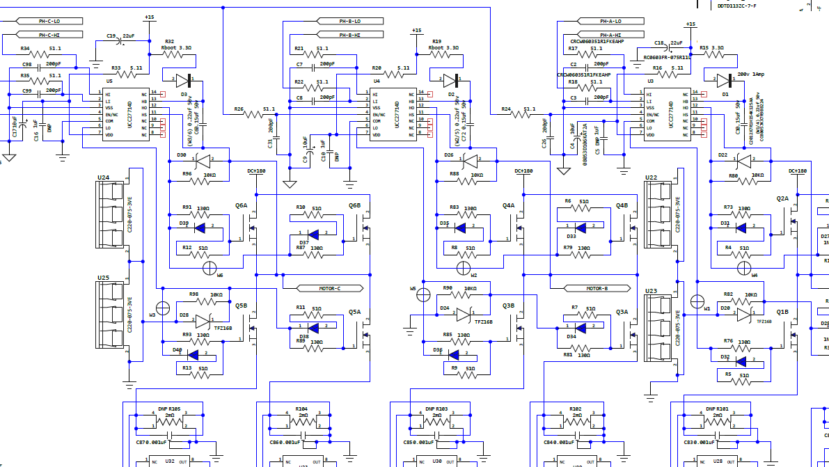
    Regarding the schematic, I see there are 2 MOSFETs in parallel each with a 12 Ohm turn on resistance, and 24 Ohm/diode turn off resistance. From a driver standpoint, there is 6 Ohms turn on, and 12 Ohms turn off. This will result in a peak turn on current of 15V/6 Ohms or 2.5A and turn off of 14.3V/12 Ohms or ~1.2A. I recall in a previous message that you were looking at a competitor part with much lower driver current than the UCC27714. Just be aware you would have to increase the gate resistances, when using the UCC27714, to achieve the lower gate drive current, and resulting slower switching times. Also, we typically see a higher turn on gate resistance than the turn off gate resistance. Is there a reason you target higher turn on gate drive current?.

    Regards,
    Richard Herring
  • Hi Richard,

    Richard Herring said:
    I think the driver in the center location may have higher voltage transients than the other 2 which may be degrading the driver internal devices.

    Problem is the 1.94v drop was noticed prior to power being applied after replacing UCC device. Some how voltage is looping back through the center IC via VDD. That is why the center UCC keeps failing under loaded conditions, switching from 12.5kHz up to 40kHz shorted HS-HO immediately in open loop commutations. The duty cycle on floating HO starts out very low (<2us) with Cboot = 0.15uf and was 1uf Cboot when it last shorted. Somehow there is reverse voltage leakage HO-HS when 3 gate drivers exist in a circuit together share VDD source even though each UCC is isolated via 51R to +15vdc. That is what stresses HO on center driver, the question is how or what in UCC design is allowing reverse voltage to complete the circuit. Seemingly we need a work around to stop phantom reverse voltage circuit forming, by adding a series diode to VDD or something? The center UCC is not statically balanced to some margin of other partner UCC's when tested via diode drop pin to pin. Very odd center UCC HS-HO reads 503mV/1.94v drop and partners are 543-548mV/0v drops. Where on earth is the other 40mV leaking  back into circuit? This is not a good thing to be seeing at all! 

    Richard Herring said:
    Regarding the schematic, I see there are 2 MOSFETs in parallel each with a 12 Ohm turn on resistance, and 24 Ohm/diode turn off resistance. From a driver standpoint, there is 6 Ohms turn on, and 12 Ohms turn off.


    Sorry posted older schematic with lower R values. Presently GTon=130ohm, GToff=51ohms was changed from 24 ohms. So 36R+12R (48ohms) turn off and 130R+6R (136Ohms) turn on.  The NFETS are not yet in parallel, being (Wn) feeds are not solder bridged nor are partner NFETS even present. The NFETs Ciss=5000pf-6650pf Max, QG=65-87nC Max and should not have shorted UCC IGPK +/-4amps (<10us PW SHORTED) there are no shorts yet the HO outputs did not hold to datasheet specification. Circuit configuration 3 gate drivers overlapping PWM slow decay, LO NFETS are acting saturated switch (>95% duty) and dead band is added only to HO last on via local update dead band synchronization. 

  • Richard Herring said:
    there is an ATE test that confirms the HO and LO driver saturation at a test current

    Obviously test or other production issues are somehow corrupting silicon integrity HS-HO. Again replaced center UCC, first testing in/out of circuit HS-HO diode drop 520mV only. Several new UCC devices were reading some kind of drop in the reverse direction HS-HO < 1.94v. The lower failure drop <1.94v UCC did not hold up under load conditions with gate drive resistors shown in below schematic. Perhaps we have been chasing a production ghost for several months slowly increasing GTon/Off resistor values to compensate for marginal UCC devices. It seems the ESD protection diode HO/HS may be cause yet all anti static precautions were taken during our handling and installation per datasheet solder pin temperatures.

    Several devices have failed mostly in center location though that seems the position we have replaced more often upon recent failures HO-HS. Haven't even populated the parallel NFETS since the UCC keeps failing well under <2.5A drive. Postmortem UCC testing point to HS-HO junction breaking down for unclear reasons other than HO pulses sometimes approach 17v, zener clamps HO-HS 16.02v. Yet all three UCC have same zener protection circuit. Also reason to reduce Cboot value as HB was quickly saturating 1uf during produce 30-50us^ pulses initial open loop commutations @12.5kHz.

    Again 40khz PWM is no issue at 24v supply yet quickly destroyed center UCC at 80v supply, 1/2 actual projected supply. We ran 180v with competition gate drivers in far worse inverter PCB conditions. The main difference now is the HO zener (Vz=16.04) was placed on NFET gate, zener (IA=10mA) 500mW never short out when HO shorts to HS. Please verify if production issues are common and what lot numbers were/are effected in the way described in this thread? UCC are manufactured in US, Malaysia or Singapore?  

  • Seemingly competitions gate driver bulletin AN6076 covers VS-HO pin break down, no longer occurring FAN7381. Oddly the center phase has far less B+ overshoot than last phase. It was hopped less parts count being required as figure 53 paints HS pin being dv/dt immune (-80 to -70v) for 100ns. The largest dv/dt peaks tend to capture on LO side drive are -10v and virtually go undetected on phase drive output.

    Simply placing Schottky diode on last phase Vmotor to COM reduced peak HS pin overshoot transients. Perhaps dv/dt current HO-HS pin should flow into COM. Seemingly further analysis reveals reverse current HS-HO (dv/dt) thus flows back into LO output versus the floating HS pin as depicted via figures 52/53 testing captures or graphs. Obviously LO internal Totem pole is immune to the dv/dt that can easily stress HS-HO junction via undocumented 3rd current path not depicted in figure 50.

    Figures 52/53 testing is very misleading as if HO driven dv/dt is constrained to HS pin when it traverses into LO side NFET drain during motor commutation. Some kind of technical brief datasheet update or Wiki report work around is required to constrain reverse Vmotor current (dv/dt) flowing out the HS pin into LO. Please explain best methods to mitigate 3rd current path, transfer HS dv/dt into LO not being disclosed in datasheet application section.