This thread has been locked.

If you have a related question, please click the "Ask a related question" button in the top right corner. The newly created question will be automatically linked to this question.

LM5045: HS1 sinking current to GND

Part Number: LM5045

Hello all,
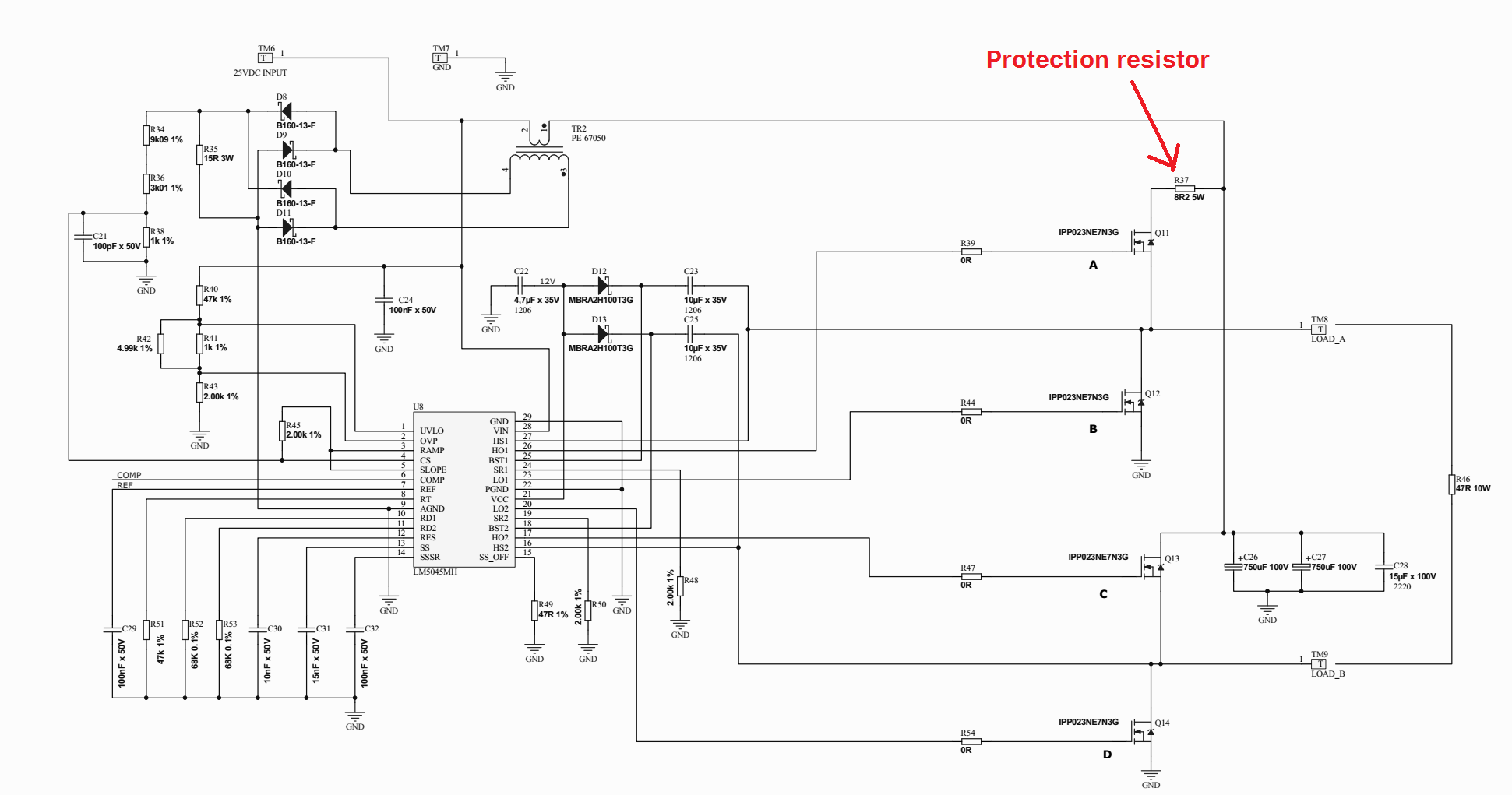
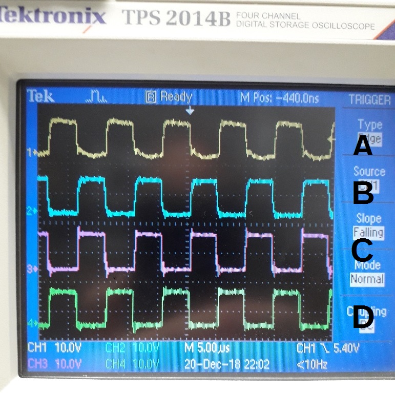
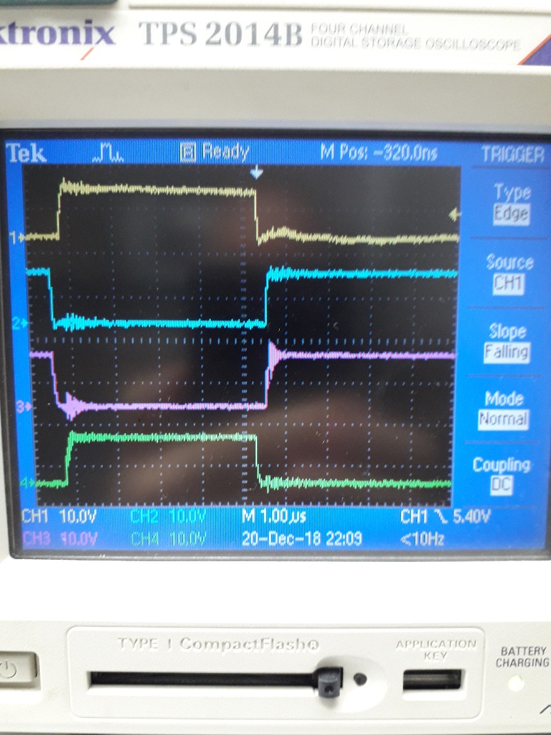
I have a DC-DC design using LM5045 with the HS1 pin sinking current to ground. HS2 pin is working properly. I have replaced the IC once and problem remains. Before replacing again I though to ask the comunity if this behavior was seen before. In order to study the problem I have installed a protection resistor of 8R2 in the drain of the high side MOSFET 1 (see schematics). Without this resistor the MOSFET burns out. With this resistor the gate drivers seems all okay. The side 2 works correctly all time. Even disconnecting the resistive load the problem remains. Its is not related to rise/fall time of transistors (that could trigger a shooting-through in some MOSFETs). As seen in the scope photo, the HS1 path seems to be grounded. In fact, the LM5045 gets hot and the voltage ramp on HS1 seems to indicate some internal resistance with thermal behavior. When the circuit is powered off I did use a multimeter to measure resistence between HS1 to ground (and HS2 to ground) and both shows the same value of 4.4Kohm. It does mean the grounding effect is an active response from the internal circuit and not just a short-circuit (internal or in the PCB). Also, both HS1 and HS2 with same resistence value seems there is no observable difference in the device's circuit. The device seems to operate correctly with all timings and responses as expected.
The COMP input is floating because I have removed the transformer and the whole secondary side is meaningless during this study. Anyway, LM5045 with COMP left open just goes to 50% duty cycle and this is okay to study it's behavior. The schematics is a simplified reproduction of the actual one to show what is in operation during this study. Including the not used circuits would only add noise to this post.
It is important to clarify this behavior happens with or without the load. Therefore the current is not passing through the Lower Side MOSFET 2. The current is also not passing through the Lower Side MOSFET 1. It is off (as seen in the picture as signal B and measured in the circuit, just to be sure).

The voltage on the load shows the correct operation when Upper SIde MOSFET 2 is on and Lower Side MOSFET 1 is on. So, even if HS1 is internally grounded, during this phase the Lower Sidfe MOSFET 1 active also grounds HS1 and therefore the issue does not affect operation.

I can replace the device again but wonder if I made some so ridiculous mistake I can't see. The IC was purchased from Digikey about 6 months ago and I believe it is not a counterfeit.

Any clues?

Thank you in advance.

Best regards,

Augusto Einsfeldt

With protection resistor in place the gate voltages seems to be correct.

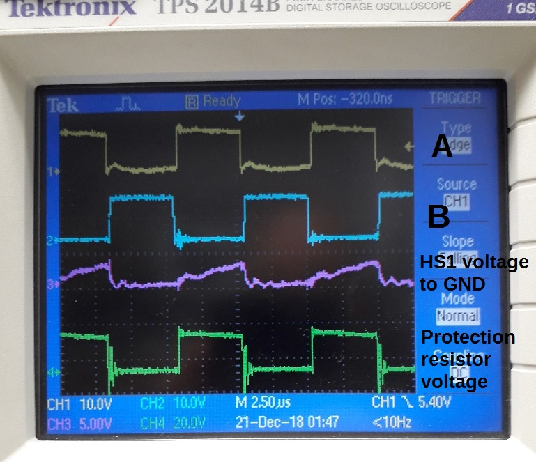
The protection resistor voltage shows the current passing in the upper MOSFET.

  • Hi Augusto Einsfeldt,
    From your information it is not clear to me why you are confident that this current is flowing through the LM5045.
    The HS1 pin is connected to Drain of the lower MOSFET and my thinking is that it may be an issue with the lower MOSFET that is not turning OFF correctly. Perhaps it is this lower MOSFET (Q12) is damaged?
    Please try to verify that the fault current is flowing through the LM5045 and is not flowing through the lower MOSFET.
    The LM5045 was released several years ago and is used in high volume in very many products. I have not heard about any issue such as the one you describe.
    Thanks
    Joe Leisten
  • Hi Joe,
    The current is flowing through LM5045. Q12 is not damaged and is switching correctly. No issues in the Lower MOSFET. I know LM5045 is not new and I am now thinking if it could be a batch problem. I have lot of experience in electronics and have spent several days digging on this problem because I could not believe the LM5045 would drive HS1 to ground. I also checked the data sheet if I could have switched pin numbers by mistake while making the symbol in the Altium Designer. (Please, note that my mention about experience was only to clarify I have checked all possible known issues).
    I thought I made some silly mistake that I could not see.
    I will replace the device and check again. But it may happens only beggining of January due to holidays here starting today.
    Thank you for your attention on this subject.
  • Hi Augusto Einsfeldt,
    One more observation.
    The capacitors that you are using to bootstrap the high side drivers (C23, C25) are much larger than recommended.
    You are using 10uF and the design example in the datasheet uses 0.1uF in this location.
    In normal steady-state operation this should not matter but when the low side MOSFET first turns on a discharged 10uF capacitor is applied directly from VCC to GND. I am concerned that the resulting charging current may cause damage either to the LM5045 device or the diodes D12 and D13. Even if it does not cause damage it is likely to pull VCC down to a level that could cause mal operation of the part.
    Have a good holiday.
    Joe Leisten
  • Hi Joe,

    Good point. Thanks for the observation. It was a wrong component selection in the library and non noticed afterwards. I am back to work now and will replace the LM5045 and reduce the capacitors.

    Best regards,

    Augusto

  • Hi Joe,

    Indeed, the bootstrap capacitors were the problem. 10uF was too much and made the LM5045 go nuts. After replacing the device and reducing these capacitors to 0.1uF the circuit started to work as expected.

    Thank you for your observation.

    Best regards,

    Augusto