This thread has been locked.

If you have a related question, please click the "Ask a related question" button in the top right corner. The newly created question will be automatically linked to this question.

TPS22946: TPS22946 Problem

Part Number: TPS22946

Hi Team,

I have serious problem with this device.

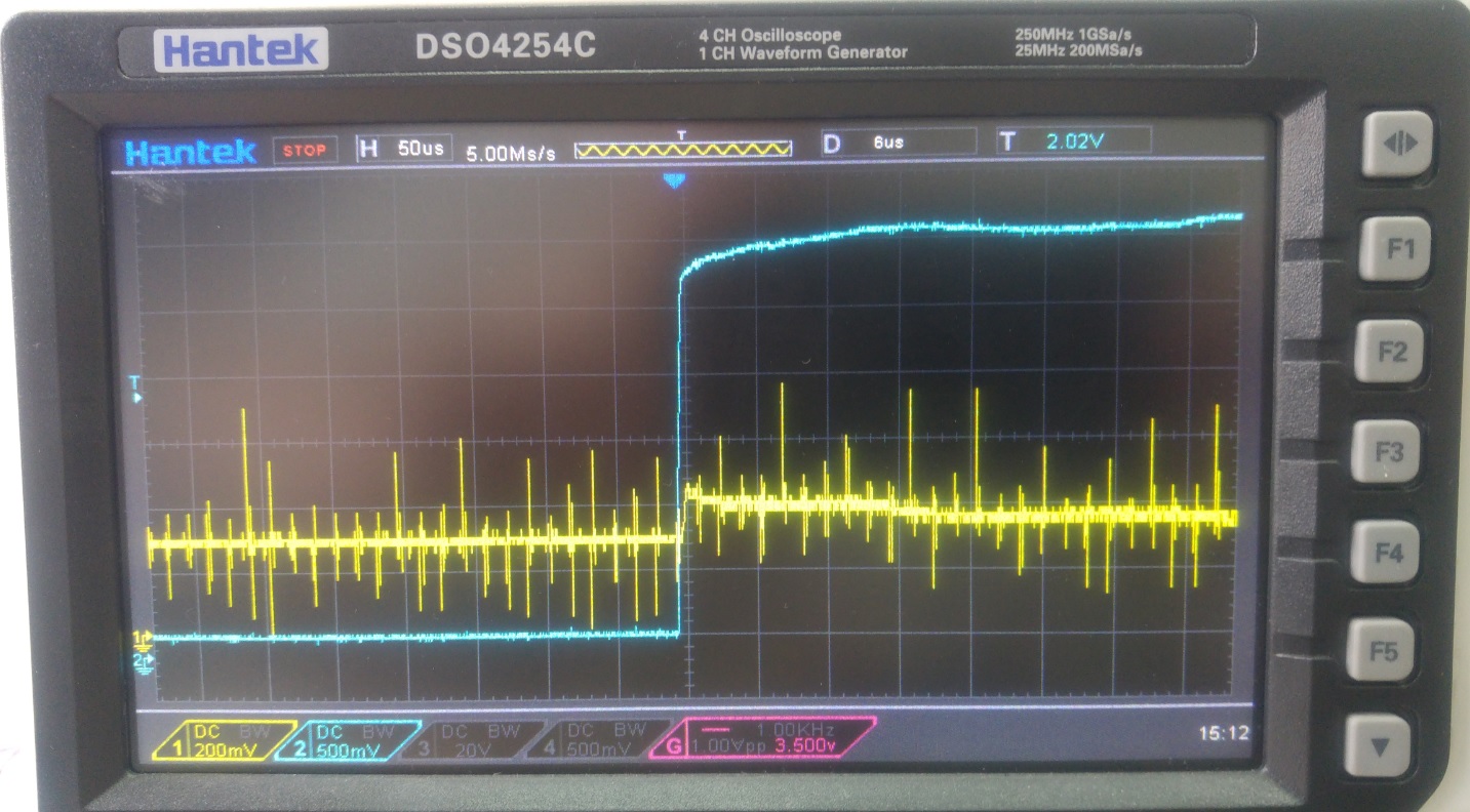
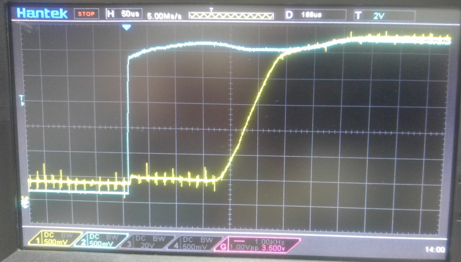
Load on VDD_SBP about 12mA and capacitance 500nF and after resistor 100Ω additional 3.3uF

Input +3.3V can be switched off and on by electronic switch.

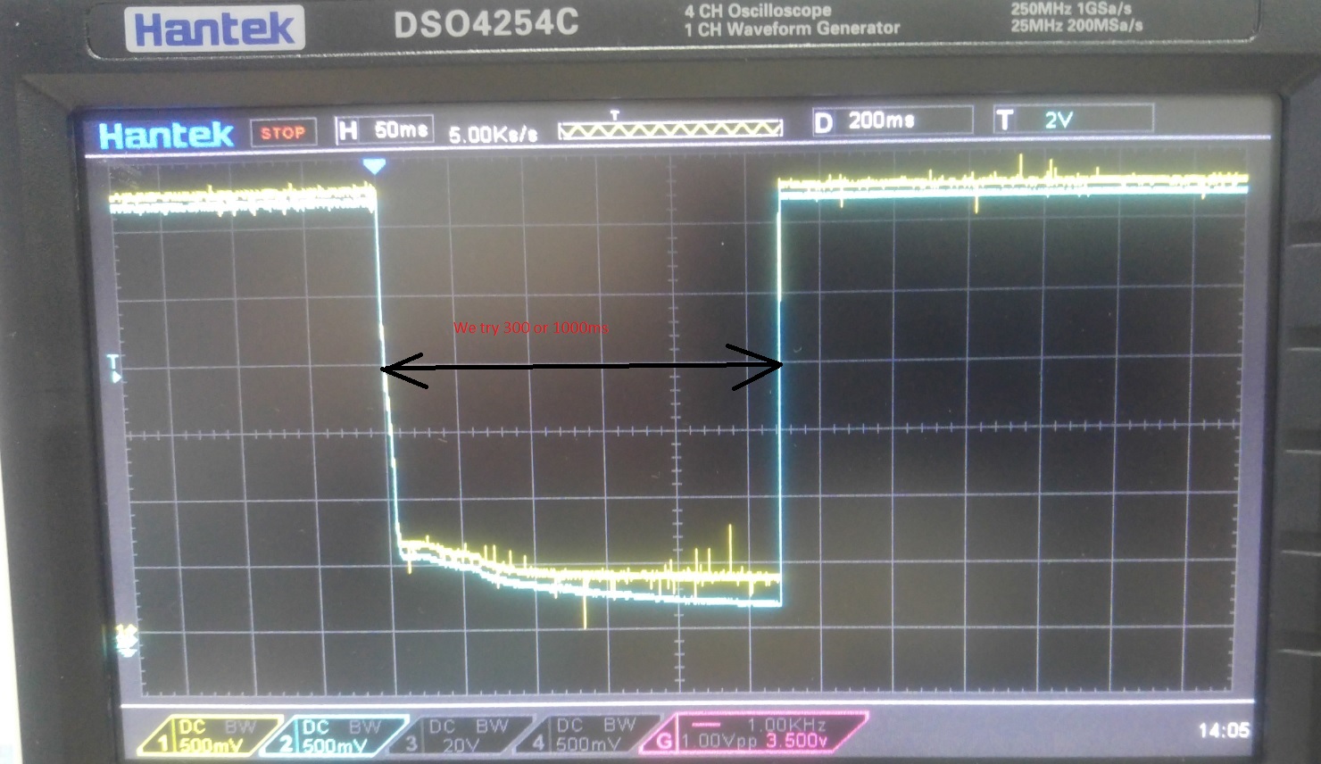
When I switch +3.3V Off and after that On with delay about 1 second on VDD_SBP I see sometimes 0.2V Looks that device is in protection mode.

Why?

What is a minimum time allowed between OFF and ON +3,3V again?

Please advise.

Issue is critical.

Thanks,

Shlomi


TPS22946.docx

  • Hi Shlomi,

    Do you see 0.2V at the output of load switch?

    Can you please provide some waveforms with input and output voltage and currents captured during this behavior?


    Regards,
    Kari.
  • Hi Kari,
    Part of problem solved. I found that 2 devices were damaged and after replacement looks ok. But still in testing.
    Now most important to me to correct my firmware is to obtain following information that I cannot find in datasheet when device connected as in on the picture:

    1. When I switch OFF +3.3V what is a threshold that voltage shall drop below that device will reset itself and will be ready to new power on?
    2. How much time voltage shall be below threshold before next power on to provide stable switch ON after that?

    Thanks,
    Shlomi
  • Hi Kari,

    Still in part of devices TPS22946YZPR I have problem.

    Replacing devices solves it.

    I remind that I switch device off, wait 300ms or 1000 ms and switch the device on by switching on +3.3V.

    On attached waveforms blue is +3.3V input and yellow is an output

    On picture TPS22946YZPR_NormalOffAndOn.jpg you can see our normal case and TPS22946YZPR_NormalOn.jpg is normal case zoomed to switch on time

    On Off300msAndProtectionAfterOn.jpg you can see that after switching input on what happen with output.

    Manual Replacing elements solves this problem but because it is BGA I do not know if it is an element problem or soldering problem.

    Please help.

    Also I remind that my two questions still open


    1.       When I switch OFF +3.3V what is a threshold that voltage shall drop below that device will reset itself and will be ready to new power on?

    2.       How much time voltage shall be below threshold before next power on to provide stable switch ON after that?

    Thanks,

    Shlomi


    TPS22946 Sch.docx


  • Hi kari,
    I still waiting for answers to this urgent issue.
    Please note that it is a discharge resistor 1MΩ between +3.3V input and ground. If I replace it to 100KOhm it looks (I am not sure) that it solves problem.
    But I do not understand why.
    Please advise for all my questions.
    Thanks,
    Shlomi
  • Hi Shlomi, 

    Thanks for reaching out on E2E! Kari has been filling in while I was away on vacation, thanks for being patient as many of us are returning from holidays. 

    After taking a look at your configuration, the issue might be due to connecting the ON pin and VIN together. When both VIN and ON are tied together, the controlled slew rate for the device cannot be guaranteed because the device has not had sufficient time to power up. Furthermore, the TPS22946 and other current limiting load switches would not be able to control the inrush current since the circult limit circuitry isn't active until the part is fully powered on. 

    If you want to keep ON connected to VIN, you can try adding an RC filter between VIN and ON. The delay time between VIN and ON should be at least the turn on time for the device (tON). Otherwise, is it possible to separate the VIN and ON input supplies?

    Thank you,

    Arthur Huang


    To find the latest information on Power Switches, visit www.ti.com/powerswitch

  • Hi Arthur,
    It is a disaster, I am in production phase. I have not faced this issue in proto builts and there is nothing about it in datasheet.
    This required PCB changes.
    Any another idea.
    Inrush in my case is not an issue because capacity on output is about 200 nF
    Thanks,
    Shlomi
  • Furthermore to my previous post on figure 22, 23 datasheet Vin and Von rise simultaneously
  • Hi Shlomi,

    If controlled slew rate isn't a concern, then connect VIN and VON is ok. Another potential concern is from soldering the BGA package. You mentioned that manually replacing the devices fixed some of the issues.

    If the incorrect nozzle force and mounting techniques are followed, this could lead to chipping and/or incorrect performance. How are you soldering the devices to your production board?

    Please refer to Mounting of Surface Mounted Devices for guidelines on soldering the TPS22946. For this device, I recommend using 120-125 gf.

    Thanks,

    Arthur Huang

  • Hi Arthur,

    Still no answers to my questions 1 and 2.

    About inrush current.

    As you can see in attached pictures when device switched on normally slew rate is more than 50us.

    But when device is not switched on normally voltage does not exceed 200mV and regarding to base line voltage raised only 100 mV and stop .

    On output of TPS22946YZPR 300nF capacitors and 3.3uF after 100Ω resistor.

    Device current limit is 30 mA.

    Is it reasonable that 100 mV can cause inrush current protection?

    Thanks,

    Shlomi

  • Hi Shlomi, 

    Looking at the TPS22946 datasheet, the TPS22946 has a 435mA current limit during initial turn on. I've estimated your turn-on time to be ~100us from your graph. Please find the calculation for your inrush current below:

    Iinrush = Cload * dv/dt

       =  3.3uF * 3.3V / 100us

       =   ~100mA

    Therefore, I don't see the inrush current limit being a factor during startup.

    Please find the answers to your questions below. 

    1.       When I switch OFF +3.3V what is a threshold that voltage shall drop below that device will reset itself and will be ready to new power on?

    [AH]: With ON connected to VIN, it is difficult to know the threshold voltage where the device will reset. Once the voltage on the ON pin goes below VIH (~1.1V), the output of the load switch is undetermined until the voltage drops to VIL (~0.4V). Once the voltage on the ON pin reaches VIL, the output of the load switch will remain at 0V.

    2.       How much time voltage shall be below threshold before next power on to provide stable switch ON after that?

    [AH]: You can use the power-on time as a good estimation, ~192us.

    Thanks,

    Arthur Huang

  • Hi Arthur,
    But 3.3uF after 100ohm without 300nf so I believe the inrush current is much below 100mA.
    Can we do conference call today or if you can call me 972-50-5263040 about this issue?
    Thanks,
    Shlomi
  • Hi Shlomi,

    Feel free to email me at a-huang@ti.com and I can send you a conference invite. Unfortunately, my schedule is pretty booked until Friday, does that work?

    Thanks,
    Arthur Huang