This thread has been locked.

If you have a related question, please click the "Ask a related question" button in the top right corner. The newly created question will be automatically linked to this question.

UCC28881: DC/DC back converter

Part Number: UCC28881
Other Parts Discussed in Thread: UCC28880

Hello,

I have the 270Vdc line, and I must make auxillary power supply 15V for logic IC.

I was recommended to use UCC28881 (back converter)

I assembled the scheme in accordance with application from DATA of the component

I applied the recommended calculator to calculate the values of all components.

Cvdd = 100nF

Rfbt = 130k

Rfbb = 10k

Cfb = 800nF (470nF parallel to 330nF)

L = 400uH

Cout = 220uF

Rout = 27k


When you turn on the input voltage 270Vdc, output voltage rises to 15V, but after 150 msec it drops to 5.5V.


What am I doing wrong?


Thanks,


Leonid

  • Hello Leonid,

    Thank you for your interest in using the UCC28881 in your application.

    Most of the text in your post is identical to that of a reply in a separate thread that I have supported on what appears to be the same issue.
    Ref: e2e.ti.com/.../2805521

    Are you the customer to which the poster (Eli) refers in his original posting on this topic? If so, I'd prefer to continue support directly with the customer (presumably you) rather than through an intermediary.
    Please verify if you are the actual source of the regulation issue with the UCC28881 of Eli's post.

    Regards,
    Ulrich
  • Hello Leonid,

    I have received confirmation from Eli that his E2E thread is the same as your thread, and I will continue to support this issue with you directly.

    With the change of components as you list above, we seem to have changed from a gross overvoltage at start-up to a gross undervoltage.

    We'll need to consider possible reasons for why the output would sag ~10V after, or during the course of, 150ms of operation.
    The component values seem to be reasonable for the application. As I mentioned to Eli previously:
    "Also, please verify that the components on the board match the values and specs of the Webench design recommendations.
    Sometimes a wrong part can be loaded even though the schematic appears to be okay."
    1. It is always prudent to make sure the prototype assembly matches the schematic design.
    2. Assuming that the parts are correct, please check to see if the 270vdc source maintains voltage after start-up. It should not be collapsing due to current limit, for example.
    3. If 1 and 2 are okay, then the feedback input (FB) must be seeing higher voltage than expected and the loop is cutting back the duty cycle to compensate. 130K and 10K are about right for ~15V output, provided that Cfb has 15V impressed across it.
    This is difficult to verify since Cfb is referenced to the switching node. You'll need to use a high-voltage differential probe to view it.
    The purpose is to see if this cap is being overcharged, possibly due to stray inductance in the pcb layout.
    4. Make sure that the board is clean of solder flux, especially around the 130K resistor and the IC input. Flux residue can sometimes absorb moisture and reduce the resistance of high-impedance networks, changing the divider ratio unexpectedly and significantly.

    I hope that one of these points can explain the undervoltage sag, and can be corrected. Please let me know what happens in your investigations. If you can provide waveforms, that may prove helpful for debug.

    Regards,
    Ulrich
  • Hello,

    Thanks for the answer. Yes, quite right, I asked this from Eli.

    In the near future I will make a measurement - how does the voltage on the FB contact behave?

    I also have a question about inductance: if I measure it at a frequency of 10 kHz, then I get 400 uH
    But at a measurement frequency of 1 kHz, I get 500 uH. Maybe it makes sense to reduce the inductance?

    By the way - Webench  recommends completely different values - Cfb = 2.2uF and L = 6.1mH. This is what I did at the beginning, but then the output voltage rose to 60V by 150 msec, then it dropped to 15V.

    Thanks

    Leonid

  • Hello Leonid,

    I ran the Webench and got the same result as you did. But I noticed some discrepancy between the inductor spec'd current (40mA) and the operating current (334mA). I suspect that the Webench algorithm begins with a CCM design (resulting in 6mH) then finds the operation to be DCM (with the high Ipp). I have sent in a notice to the Webench team to investigate this and a few other issues that I found.

    Meanwhile, I also went through the Excel calculator tool in some depth (though not exhaustively) comparing to the datasheet procedure and found that the Calc tool also has a bug: the result for Cfb is missing a factor of 1/10 (per Eqn 17 of the DS).
    So Cfb should be about 88nF, not 880nF. This would make the response about 10 times slower than it should be.

    Please reduce your Cfb cap from 800nF to 82nF, and see if the strange voltage gyrations at start-up go away.

    To answer your other questions:
    The voltage on FB should resemble (if you could probe it with an HV diff-probe) that of Vfb in Figure 13, page 13 of the DS.
    It may not have perfectly straight lines, but it should be of similar asynchronous timing.

    I would measure the inductor at 10kHz. An LRC meter may not have enough drive capability at 1kHz with low inductance and might saturate its current and obtain inaccurate results.

    By the way, can you please expand on the overall specifications for this project:
    For a DC input, what is the very minimum and very maximum voltages over which it must operate?
    Will the output current be a fixed 20mA or have variable loading? If variable, what is minimum external load?
    What are your output voltage limitations? Min, max, typ = 15V, etc. Allowable ripple voltage?

    Finally, 15V at5 20mA is a very light load for the UCC28881. I suggest to consider using the UCC28880 in order to reduce the maximum short-circuit current that might result. 0.3W is well within the UCC28880 capability, too.

    Regards,
    Ulrich
  • Hello, Ulrich,

    Thanks for your reply. I'll try to reduce the capacity Cfb now and then write about the results.

    As I said before, I need this scheme to improve my finished product, which we have been producing for several years: there is a product that works on voltage 270Vdc, and it has several logic circuits that are powered by 15V. In the development process, due to lack of time, I used a 15kilohm/5W resistor and a 15V diode zener. The customer complained of excessive heat, so I'm looking for a solution with less power loss.

    Input voltage - 180-290V with transients of maximum 330V/100msec, the current - 20-25mA continues.

    Thanks,

    Leonid

  • Hello,
    I made measurements with a capacitor Cfb = 88nF
    The output voltage first rises to 15V, and after 150 ms it drops to 6.4V
    Nothing happens.
  • Hello Leonid,

    I'm sorry that you are continuing to have problems with your application. I'll try to help you solve them.
    Thank you for the information you provided so far; I'm going to request more, including some waveforms if at all possible.

    But first, I'd like to clear up a discrepancy:
    As I understand it, your output spec is 15V (let's assume +/-5% based on earlier zener design) with a 20mA load (25mA max, per above posting.) With 180V minimum input voltage and 15K dropping resistor, the highest current possible is (180V-15V)/15K = 0.011A. Even if the 15K were shorted to GND, there would only be ~12mA through the resistor, so this could never provide sufficient current to the load based on your spec. Even at 290Vdc, there is only 18mA through the resistor; still not enough for the max load.
    When you mentioned the input range is 180V to 330V, then say the current is 20-25mA continuous, do you mean that the high-voltage "input" current is 20-25mA, or that the 15-V "output" current is 20-25mA?

    This discrepancy doesn't affect the problems encountered while using the UCC28881, but it does raise questions about what the true output specification really is. Please quantify the minimum and maximum values for Vout and Iout. Also, can you tell me if the output load draws any significant peak currents well above the average? If so, for what duration?

    Now back to the buck regulator:
    1. I recommend to change from UCC28881 to the UCC28880, which has a lower peak current limit, more appropriate for your load level. This will result in requiring a higher inductance (1.2mH) plus a few other component value changes.
    But I assume that you may not be able to readily obtain samples of the UCC28880, so I'll continue to debug the UCC28881 that you do have.

    2. Given that the Cfb time constant does not affect the response that you are getting, I am thinking that an alternative explanation for the output sag after 150ms could be from a thermal problem.
    The freewheeling diode used from the inductor to "GND" should be a high-voltage ultrafast diode. What part number are you using for this part? Actually, please tell me the part numbers for both diodes, the free wheeling one and the feedback one).
    The datasheet recommends reverse recovery times of <75ns for DCM applications (which this one is).
    A slower diode will have higher reverse recovery current which will heat up the junction which increases the recovery time, which heats it more, which results in a spiraling thermal runaway. If you are using a slow diode in the freewheeling position, this may account for the voltage sag after ~150ms.

    3. More of a long-shot could be that the inductor is saturating and leading to current limit operation.
    Please provide the specifications (or catalog part number) of the inductor that you are using.

    However, I am only making guesses, based on the information that I have available.
    If you can provide waveforms of the start-up period, that can help a lot to figure out exactly what is going on.
    Ideally, I'd like to see:
    Vout at 5V/div, Vgnd (pin1,2 of the IC) at 50V/div, Iind (inductor current) at 100mA/div; time sweeps of 20ms/div and faster.
    The 20ms/div sweep can capture the entire start-up sequence.
    The faster sweeps should capture one or two switching cycles at the beginning, when Vout is ~15V, and a few cycles near the end, when Vout has dropped to ~6V. I do not know what the specific "us/div" sweep rates should be; sufficient to capture one or two switching cycles.

    I hope that you have access to a current probe. This would be very helpful.
    Don't forget to provide the information about the diodes and the inductor.

    Regards,
    Ulrich
  • Hello,

    You are right, the current consumption for the logic is now 10mA, but in the future I plan to change the design, so I need a power source with a current of 25mA.

    As for my problem with UCC28881 - I do not understand: on all contacts of the chip  the voltage behaves the same with respect to the "minus". It seems that the chip burned. But he did not burn

    I use diodes CMMR1U-06

    Thanks

    Leonid

  • Hello Leonid,

    Thank you for the additional information. Every little bit helps. However I really do need all of the information that I requested in my last post. Please review it and let me know what you can and cannot provide, to help solve this problem.

    The CMMR1U-06 diode spec lists 100ns for reverse recovery time, which is a little slower than the datasheet recommendation. Since this application should be running in DCM, I don't expect it to be a big contributor to reverse recovery loss (which can be a big problem in CCM applications). But it is prudent to check it. This can be verified by using a current probe, if you have one.

    I am a little confused by your comment " on all contacts of the chip the voltage behaves the same with respect to the "minus". It seems that the chip burned. But he did not burn ".
    If I interpret this correctly:
    a. the "minus" is the negative reference rail, at the anode of the freewheeling diode D1.
    b. the IC appears to have failed because all the pins voltages appear to be the same, yet switching still happens and some power is generated.

    If I understand correctly, I think that you are probing the IC pins with respect to the negative rail, and these pins are all switching up and down between "minus" and "plus" of the input. Since the IC will have very low voltages on its pins with respect to its GND pins (except for HVIN and DRAIN), and because the input voltage is a 270Vdc, the low pin voltages are superimposed on the high input voltage and you will not be able to distinguish the pin voltage from the input voltage. To do this, you will need to use a high-voltage differential probe, referenced to the IC GND pins.

    However that will not be necessary. We can assume that, if the input pin of the inductor is switching, then the IC is functioning.
    We need to look at that switching pattern to look for clues as to what the IC is doing and figure out why it is doing that.
    So I request again, if you can please provide the waveforms that I mentioned above (voltage measured with respect to the output "minus"), it will be a big help to diagnose the problem. And also provide the other information that I requested.

    Thanks and Regards,
    Ulrich
  • Hello Leonid,

    It has been a week since my last post and I haven't heard any update from you.
    Therefore, I need to close out this thread.

    I hope you are making progress on your end.
    If you need further support, please open a new posting and please provide all the information necessary for understanding and diagnosing the problem.

    Regards,
    Ulrich
  • Hello,

    I apologize for the late reply, was busy with other things.
    I tried to change both the chip and the type of diodes. Nothing happens. All the same - when turned on, the voltage at the output of 15V, after 150 milliseconds drops.

    I tried to look at the problem more systematically. I am looking at the component structure diagram on page 9, and I don’t understand how GATE gets its increased voltage so that FET opens?

    It seems to be a bootstrap - a diode with an anode on pin 5 and a cathode - on pin 4, but this is not mentioned in any application!

    Maybe this component is generally not suitable for the input voltage of the DC? Only AC?

    Thanks

    Leonid

  • Hello,

    I apologize for the late reply, was busy with other things.
    I tried to change both the chip and the type of diodes. Nothing happens. All the same - when turned on, the voltage at the output of 15V, after 150 milliseconds drops.

    I tried to look at the problem more systematically. I am looking at the component structure diagram on page 9, and I don’t understand how GATE gets its increased voltage so that FET opens?

    It seems to be a bootstrap - a diode with an anode on pin 5 and a cathode - on pin 4, but this is not mentioned in any application!

    Maybe this component is generally not suitable for the input voltage of the DC? Only AC?

    Thanks

    Leonid
  • Hello Leonid,

    I completely understand about being busy. Aren't we all?

    Concerning the component input suitability: Both the UCC28881 and UCC28880 (and virtually all other PWM converters) only work from a DC source, actually. AC inputs are rectified to DC and the conversion plant is done from DC to DC.
    The terms "off-line" and "AC-to-DC" describe the overall conversion between power source and load, but the actual converter is a DC-DC stage, preceded by a rectifier (half-wave, full-wave, or PFC).

    Concerning the diagram on page 9:
    I assume you are referring to the Functional Block Diagram on page 9 of the UCC28881 datasheet.
    The GATE driver stage, and all of the other blocks within the IC, are all powered by the VDD regulator (LDO). This LDO is filtered with an external cap from pin 4 to pin 1, for LDO stability and to store charge for the gate-drive. The LDO receives its power through a limited current source from the pin 5 HVIN input (connected to the high voltage positive rail).
    This HVIN current must flow in a closed path, and the return path (back to the high voltage negative rail) is initially through the output inductor and the output cap. At start-up, Vout = 0V, so the load is not involved.
    After switching starts, the inductor current forces the freewheeling diode D1 to conduct, so the HVIN current path continues to flow through D1 to GND while D1 is on. The HVIN current is generally much lower than any load current so it does not affect output regulation when D1 is off.

    So there is no internal bootstrap diode... in a certain sense the entire IC is its own bootstrap device.

    Concerning the on-going problem of voltage collapse after 150ms, I must again emphasize the importance of providing the waveforms and other information that I requested a few replies ago. No one can figure this out without them.
    To be blunt about it, we are looking for a problem in your implementation, not in the IC. We have shipped millions of this part used in dozens of commercial products worldwide and they all work exactly as expected. We need to find out what is peculiar about your implementation that results in the symptoms you described. And this requires analyzing the waveforms and other info requested. Also, I recommend to verify that your load is a fixed 10~20mA load. If you are using an active circuit as the load, there may be high-current transient conditions at start-up much greater than the average. If this can't be verified, I suggest to first debug this converter using a simple 1.5Kohm, 1-Watt resistor. That will eliminate any unknown load swings from an uncharacterized active circuit.
    Please review my previous requests and provide as much of it as you can, or my efforts are futile.

    Regards,
    Ulrich
  • Hello Leonid,

    Seeing no recent activity on this topic, I need to close out this thread.
    If you need further support and can provide the information necessary to facilitate that support, you can reopen this thread or start a new one.

    Thanks,
    Ulrich
  • Hello,

    I replaced the inductor with a shielded one, and the circuit began to work. But the output voltage is unstable. And when the input voltage rises to 130V, the output voltage is distorted. Can I attach screenshots?

    Thanks

    Leonid

  • Hello Leonid,

    Yes, please do attach screen shots.  There is a roll-over link that you can click on to enable attachments of files and special text formatting.

    I'm not sure what it looks like to you, but on my display there is a hot link entitled "Insert Code, Attach Files and more..." located at the bottom right of the dialog typing box.   Click on that and the typing box will reformat to show a number of available text features.  In the middle of the bottom row of features is a "paperclip" icon which will allow you to attach external files to your post.   

    As in my previous replies, please provide as much information as possible, such as input and output test conditions, "big picture" screen shots as well as detailed cycle by cycle screen shots so we can get a good idea of the problem behaviors.  Also please ensure that the resolution is high enough to read the scope setting numbers.  Fuzzy screenshots are difficult to work with and require follow-up clarification.

    Thank you,
    Ulrich

  • Hello,

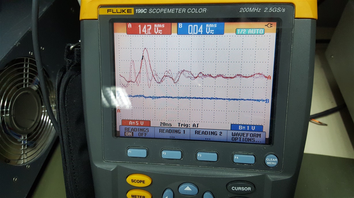
    In first picture we see the behavior of the output voltage at an input voltage of 70 - 130V. The output voltage is close to what I need - 15 volts, but sometimes short peaks of overvoltage up to 25V.

    Unfortunately, I can not attach more than one image in one message, so I will send the second image with another message

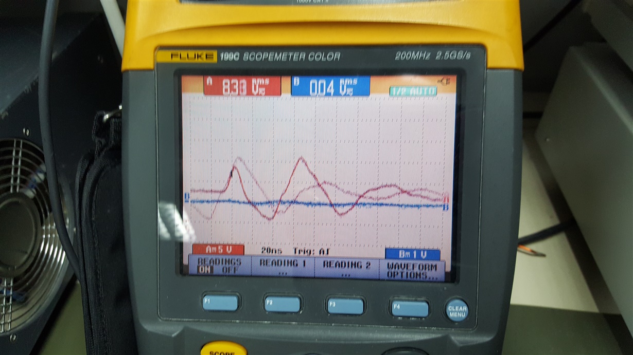
  • This is what happens when the input voltage reaches 130V

    Change happens abruptly.

    I hope this gives some information to think about.
    In addition, I ordered the evaluation board

    Thanks,

    Leonid

  • Hello Leonid,

    Thank you for posting the 2 screenshots. They are a good start. The time scale shows 20ns/div.
    Therefore, my first impression of the peaking voltages is that they are noise induced on the scope probes during switching events.
    I think such switching noise pulses can be ignored. I suggest to scale the time sweep much longer (100us/div, 1ms/div, 10ms/div, etc) to get a view of the average output voltage behavior over time from start-up to steady-state. Those peaks will be switching noise superimposed on the average Vout. You may be able to filter them out with bandwidth limit and/or lower sampling resolution (say 20ns/sample or less).
    These can be avoided using the tip-and-barrel probing technique (ref: training.ti.com/engineer-it-how-test-power-supplies-measuring-noise and barrel probing&tisearch=Search-EN-Everything )
    If the high peaks are still there after probing this way, then we'll have to address them with more concern.

    This does not explain why Vout falls to ~8V when Vin > 130Vdc.
    One possibility is that as Vin increases, so does the di/dt through the output inductor. Maybe at ~130V, the di/dt gets fast enough to couple noise into the FB pin which may be disrupting the feedback signal. If the rising di/dt induces a rising dv/dt on the FB signal, it will cross the 1V threshold too soon and cut back the duty cycle. This could be the cause of the output voltage drop.

    Please make some screen shots of Vout over many milliseconds from start-up to steady-state.
    Always be sure to list the test conditions (Vin, Iout, etc.) with each capture.
    If there is noise coupling from the inductor into the FB network, it could be a layout issue.
    Can you also include a photograph of your prototype board to show the component placement and interconnections, please?

    You should be able to attach more than one file to each posting. Just keep using the paperclip Icon for each file. I don't think that you can attach a set of files at one time. I think each file must be attached individually.

    Regards,
    Ulrich
  • Hello Leonid,

    Have you been able to make any more measurements, or have you resolved the regulation issues?
    If not, I'll be able to help you much better if you can provide the data and waveforms that I have been requesting.
    Otherwise it may amount to a lot of guessing without a basis for direction.

    Regards,
    Ulrich
  • Hello,

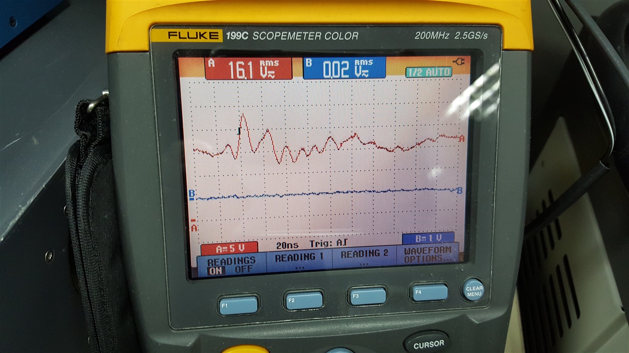
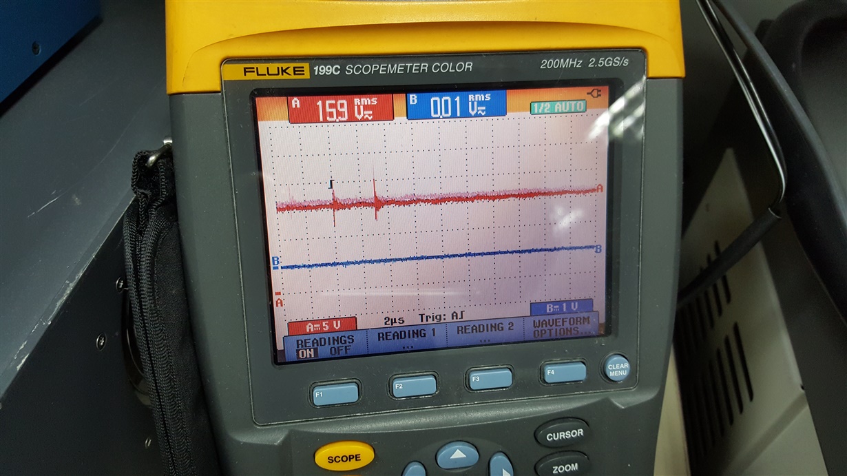
    As you saw, measurements on an evaluation board showed similar voltage behavior.

  • Hello Leonid,

    The waveform on the 20ns/div scale is just switching noise, picked up by the scope probe GND "pigtail".  It is of no concern.

    The waveform on the 2us/div scale shows that same switching noise superimposed on a clean 15-V level. 

    The noise amplitude will be much reduced if you make the measurement with the "tip & barrel" probing technique, which eliminates the GND-wire loop area of the probe.  At this point, I don't see any problem.  There will always be some residual switching noise due to output capacitor ESR and mostly from high di/dt through the cap's ESL.  Paralleling more caps will reduce it, but you don't need to do this unless the noise is causes system interference.  

    If it is merely visibly objectionable, then it can become unnecessarily complicated and expensive to eliminate completely.

    Regards,
    Ulrich


  • Hello,

    That is, do you think that such voltage I can safely connect to my logic circuits?

    Thanks

    Leonid

  • Hello Leonid,

    From the waveform that you provided, it can be seen that the DC level is clean and stable over the 20us interval shown, except for 2 switching noise pulses. This noise is most likely pickup by your scope probe GND wire loop and the true peak-to-peak amplitude at the output capacitor is not actually as high.

    From your previous postings and descriptions, I will assume that the 220uF electrolytic output capacitor is the only capacitor that you have on the output. I recommend that you add a few additional ceramic capacitors in parallel with the 220uF cap in order to better bypass the high di/dt edge of the switching current and minimize noise peaks due to Cout ESL.
    I suggest adding a 1uF, 50V multi-layer ceramic capacitor (MLCC) and a 0.1uF, 50V MLCC, both with X7R dielectric characteristics.
    These small caps will have very low ESR and ESL and will help absorb switching noise over a range of high frequency harmonics.

    This should be enough noise filtering to confidently apply the 15V output to your logic.
    If you feel that this still is not enough, you can further add a series inductor of 1uH followed by another 1uF cap to GND to effect a high-frequency LC filter on the output. The feedback network for the FB input should remain connected to the larger 220uF Cout.

    As I mentioned much earlier, your output current spec in the range of 20-30mA is quite low, especially for the UCC28881.
    Again, I suggest to change to the UCC28880 to better fit your application power level and to reduce the maximum overload current level.

    Regards,
    Ulrich