This thread has been locked.

If you have a related question, please click the "Ask a related question" button in the top right corner. The newly created question will be automatically linked to this question.

LMZM23600: Wrong dimension in Thermal Resistance vs Board Copper Area?

Part Number: LMZM23600

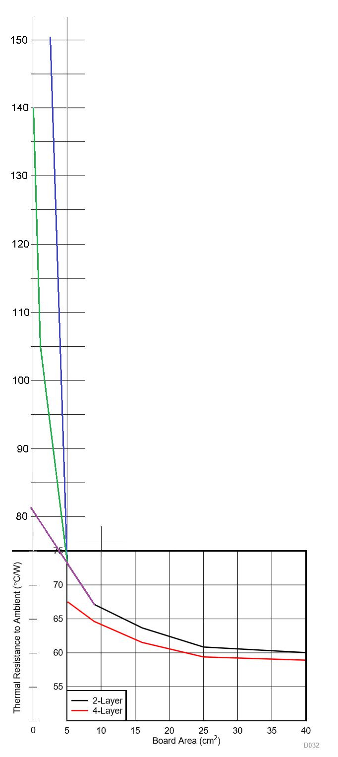
In the datasheet, Figure 7 and Figure 69. Package Thermal Resistance vs Board Copper Area, No Air Flow both express the Board Copper Area in square CENTImetres.

Could you please confirm if this is correct or that this should be square millimeters (which makes way more sense)?

  • Hi Jurjen,

    The centimeter units are correct in that figure. If you wanted a thermal resistance of 62C/W using a 4Layer board you would need a minimum copper area of 20cm^2 = 2000mm^2 = 44.7mm x 44.7mm board. Normally a device is applied to a 100mm x 100mm double sided PCB similar to the datasheet description for the LMZ31503 Footnote 2 . However this was not applicable to customer design so we created a thermal design table that would help illustrate the practical copper area the customer would need for a particular thermal resistance value. 

    Regards,
    Jimmy 

  • So, following the remark "TI recommends an unbroken GND plane or GND area of copper on the top and bottom layers", the actual required size for this minitiature device is at least 50 times bigger than its own size?? (5 cm^2 instead of about 0.12 cm^2)

    Or do i miss something?

  • Hi Jurjen,

    In your case 0.12cm^2 comes out to be 0.346 cm x 0.346cm which is roughly 3.46mm x 3.46mm. The device itself is only 3.8mm x 3mm.

    From my previous reply, say you take 63C/W you would need a copper area of 20cm^2 which comes out to roughly 45mm x 45mm board. This is correct and is based on actual thermal board testing done using different copper area and several LMZM23600 ICs.

    Regards,
    Jimmy
  • I have a PCB with total area of 10 cm^2.

    The LMZM23600 is 3.8mm x 3mm, so about 0.12cm^2. I thought: that is really "optimized for ... applications with space-constrained needs" !! I need that.

    But then, it requires 20cm^2 cooling area (or at least 5 cm^2) ... that is NOT space-constrained, it's HUGE and makes me think this device is absolutely useless for applications with space-constrained needs.

    Hence: am I missing something? Why would TI design such small components if they require such huge cooling area??

    EDIT:

    Do you have data for the thermal resistance for copper areas smaller than 5 cm^2?

    I'm expecting to need 0.35 Amps at 5V, with 36V input (worst case), acc Figure 10, the power dissipation is about 0.35W.

    Max ambient temp is 35 degr C, max Operating junction temperature is 125 degr C, so i would need a thermal resistance of (125-35) C / 0.35W = 257 C /W

  • Hi Jurjen,

    In this case you are running 36Vin to 5Vout conversion at 0.35A with a maximum ambient of 35degC. The data shown in Figure 69 are actual lab bench thermal readings. Though the graph does not include any board area less than 5 cm^2, we can extrapolate a rough idea of what the board area should be for less than 5cm^2 Looking at the graph it is similar to an exponential decay. I'd expect no more than 150C/W at 2.5 cm^2.

    Since you are running relatively low power dissipation application of 0.35W and low ambient temperature of 35 degC I don't think the need for a big copper area is warranted here. Following the datasheet equation you would need to design a board with less than 257 C/W which with extrapolation of the graph I don't think would be an issue for you unless you are planning on making the PCB area as small as the nano module itself. I can go back to the graph and get the equation that would best fit the exponential decay patterned curve you see in Figure 69 to get a more specific number for you.

    If you had a specific copper area in mind, I can run this by the graph to see if it falls within expected extrapolated range of the thermal resistance below 20mm x 20mm. In short with your application requiring a board size with thermal resistance lower than 257C/W I don't think you should see much issues designing a board smaller than 20mm x 20mm.

    Regards,
    Jimmy

  • I already tried extrapolation.

    Mathematical extrapolation

    Looking where the curve in Figure 69 has 'sharp' bends, it seems the following datapoints have been used for the 2-Layer PCB:

    4 73
    9 67
    16 63.5
    25 60.75
    40 60

    My best fit through these 5 points would be: R_theta = 59.85 + 22.875 * exp( -0.126 * A ), with A the copper area in cm^2.

    Shrinking the copper area A to zero yields a maximum R_theta = 59.85 + 22.875 = 82.7 C/W

    but, I question this best fit, because of the low number of datapoints in the relevant area (between 0 to 10 cm^2) which really determine the curve.

    Graphical extrapolation

    I neither can easily make a good graphical estimation. I also added your "no more than 150C/W at 2.5 cm^2.", which indeed seems quite high (note that R-theta in the Figure 69 starts at 50 C/W).

    I think i'll just try my current design

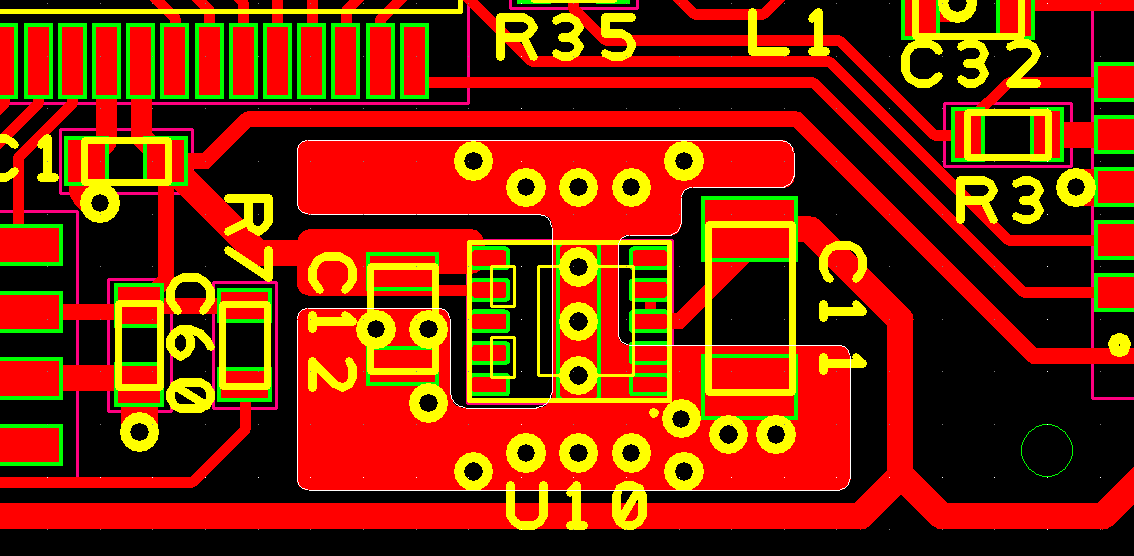
    which has a top copper area of 0.45 cm^2 and a bottom copper area of 10 cm^2 (but i expect only 2 cm^2 of this bottom copper area really contributes in lowering the R-theta).

    If the device reallyneeds a bigger top copper area (and so, pushing other components away from it and therefore forcing the PCB dimension to increase), I'll better look a solution that makes its claim for space-constrained true...

    In that case, i'd recommend TI to show the whole truth in the picture "Single-Sided Layout Solution Size 24-V to 5-V, 0.5-A DC/DC Converter" at page 1 of the datasheet.

    Because the shown solution size is at most 10 mm x 7 mm.

    Ow, and also the text in Features: 27-mm2 Solution Size With Single-Sided Layout

  • Hello Jurjen,

    Thank you for your suggestions. Perhaps we should highlight a link to the thermal design section of the datasheet.

    The board area occupied by the LMZM23600 solution is very small. As you have seen, only an input and an output capacitor are needed to get a 5Vout design. Thermal design is an important part of any power converter design. Usually the PCB copper is utilized to dissipate the power loss from the conversion process. The amount of necessary copper will vary with the application conditions (e.g. input voltage, output voltage, output current, ambient temperature, other hot components on the PCB, etc.). Section 11.1.1 of the datasheet tries to highlight this and provide some guidance on this.

    With that said, for your design it looks like the power dissipation is around 0.35W. Based on your conditions, you can have as high as ~250C/W of thermal resistance before the device reaches the maximum of 125C. If you have 10cm^2 of bottom GND copper, I feel that should be enough to achieve this thermal resistance.

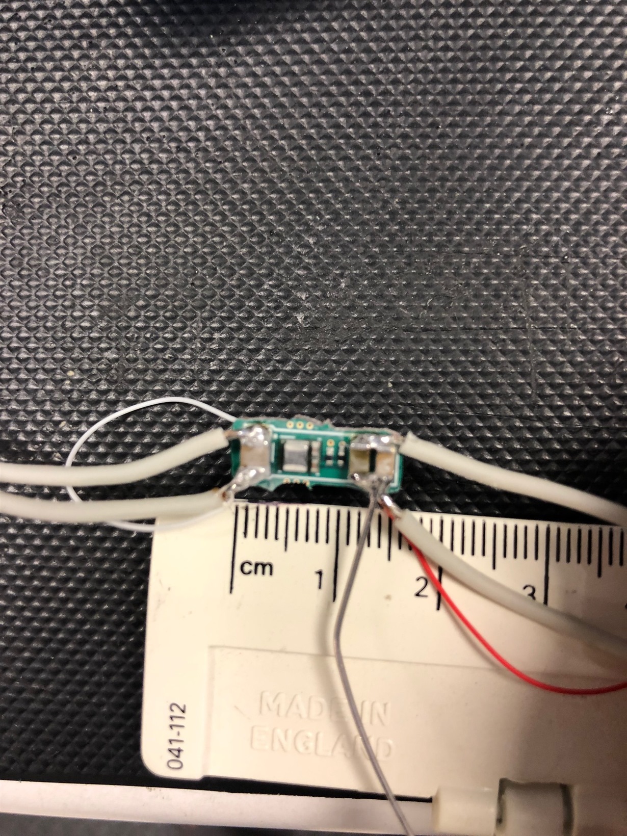
    Here is one example where we trimmed the evaluation board PCB of the adjustable output voltage version of the device to the following dimensions:


    With this board size and 0.5W of dissipation in the package, the temperature of the device reached close to 75C at room temperature:

     I hope this additional information will be helpful. 

    Cheers, 
    Denislav