This thread has been locked.

If you have a related question, please click the "Ask a related question" button in the top right corner. The newly created question will be automatically linked to this question.

BQ40Z50-R1: In-correct FCC

Part Number: BQ40Z50-R1
Other Parts Discussed in Thread: BQSTUDIO

Hi,

We have a battery using BQ40Z50-R1 installed in our system for over 6 months, but the battery has never gone thru a complete charge/discharge cycle (Cycle count = 0) since our system operates with AC plugged in.

The FCC/RMC dropped to 3482mAh (design capacity is about 8100mAh), and so we have battery fault alarm since our system check the FCC for valid range of 6000mAh - 10000 mAh.

I removed the battery from the system and set it on the table, and starts logging the information with just  EV2300/BQStudio. The FCC recovered to about 7800mAh after about 5 hours (according to the log information).

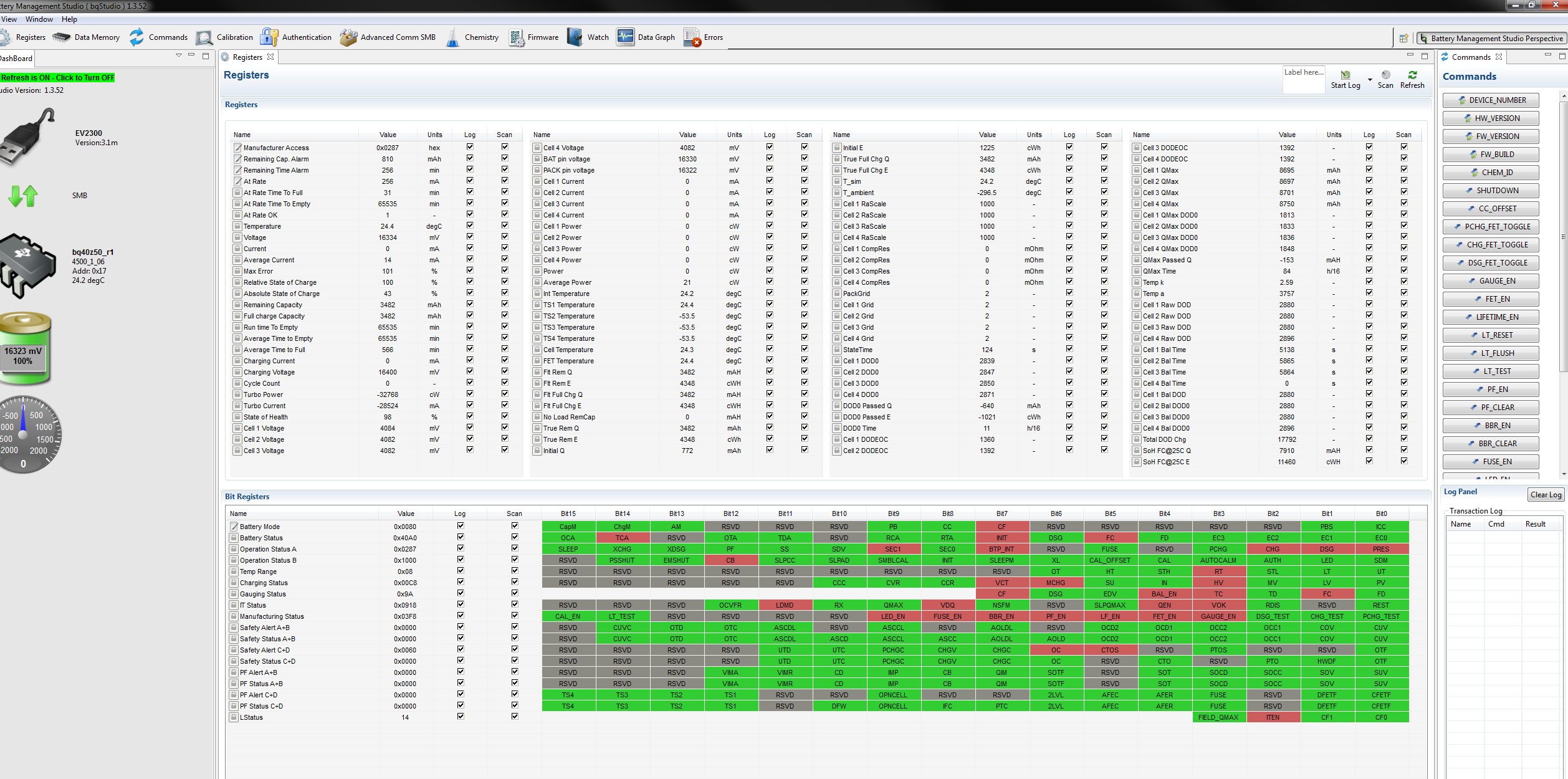
I notice that before the battery recovered, the BatteryStatus(DSG) bit is 0, the ITStatus(REST) is also 0. The T_ambient is -296.5C. Max Error = 101%. T_sim = 24.2C

When the battery recovered,  the BatteryStatus(DSG) bit is 1, the ITStatus(REST) is also 1. The T_ambient is 18.6C. Max Error = 101%. T_sim = 17.9C

Please note that this battery still have Max Simulation Iterations set at 50, not 30. The battery was also not seal.

Please see attached files.

Thank you,

Phuoc

Log File - Simplified.xlsx

  • I will be able to look into this and reply back by Thursday evening.
  • Hi Batt,

    Is there any update for this issue ?

    Thanks,

    Phuoc

  • FCC recovering is expected upon relaxation. Why did you change max simulation iterations? Those are internal parameters that are not expected to be changed. Please change it to defaults and then reset your gauge. Once you perform a learning cycle again they will be optimized.

    Also can you please upload your gg file or srec? It's much easier to analyze with that.
  • Hi Batt,

    Please see gg file. Our Battery vendor set the max simulation iterations for us at 50, and now they recommend to 30. We have not made the change to this battery yet. We understand the FCC recovered after rest period, and a full learning cycle would also help to optimized.

    However, we are interested how did the FCC reduced to about half of its design capacity.

    Can you help to provide the possibilities ?

    Thank you,

    Phuoc

    * Texas Instruments Data Flash File				
    * File created Thu Jan 03 14:27:30 2019				
    *				
    * Device Number 4500				
    * Firmware Version 1.06				
    * Build Number 36				
    * Order Number 0				
    *				
    * bqz Device Number 4500				
    * bqz Firmware Version 1.06				
    * bqz Build Number 36				
    *				
    * Field Order: Class name	 Subclass name	 Parameter name	 Parameter Value	 Display Units
    Calibration	Voltage	Cell Gain	12132	-
    Calibration	Voltage	Pack Gain	49559	-
    Calibration	Voltage	BAT Gain	49001	-
    Calibration	Current	CC Gain	1.028	mOhm
    Calibration	Current	Capacity Gain	1.028	mOhm
    Calibration	Current Offset	CC Offset	0	-
    Calibration	Current Offset	Coulomb Counter Offset Samples	64	-
    Calibration	Current Offset	Board Offset	0	-
    Calibration	Current Offset	CC Auto Config	7	hex
    Calibration	Current Offset	CC Auto Offset	0	-
    Calibration	Temperature	Internal Temp Offset	-3.2	°C
    Calibration	Temperature	External1 Temp Offset	-1.6	°C
    Calibration	Temperature	External2 Temp Offset	0	°C
    Calibration	Temperature	External3 Temp Offset	0	°C
    Calibration	Temperature	External4 Temp Offset	0	°C
    Calibration	Internal Temp Model	Int Gain	-12143	-
    Calibration	Internal Temp Model	Int base offset	6232	-
    Calibration	Internal Temp Model	Int Minimum AD	0	-
    Calibration	Internal Temp Model	Int Maximum Temp	6232	0.1degK
    Calibration	Cell Temperature Model	Coeff a1	-11130	-
    Calibration	Cell Temperature Model	Coeff a2	19142	-
    Calibration	Cell Temperature Model	Coeff a3	-19262	-
    Calibration	Cell Temperature Model	Coeff a4	28203	-
    Calibration	Cell Temperature Model	Coeff a5	892	-
    Calibration	Cell Temperature Model	Coeff b1	328	-
    Calibration	Cell Temperature Model	Coeff b2	-605	-
    Calibration	Cell Temperature Model	Coeff b3	-2443	-
    Calibration	Cell Temperature Model	Coeff b4	4696	-
    Calibration	Cell Temperature Model	Rc0	11703	-
    Calibration	Cell Temperature Model	Adc0	11703	-
    Calibration	Cell Temperature Model	Rpad	0	-
    Calibration	Cell Temperature Model	Rint	0	-
    Calibration	Fet Temperature Model	Coeff a1	-11130	-
    Calibration	Fet Temperature Model	Coeff a2	19142	-
    Calibration	Fet Temperature Model	Coeff a3	-19262	-
    Calibration	Fet Temperature Model	Coeff a4	28203	-
    Calibration	Fet Temperature Model	Coeff a5	892	-
    Calibration	Fet Temperature Model	Coeff b1	328	-
    Calibration	Fet Temperature Model	Coeff b2	-605	-
    Calibration	Fet Temperature Model	Coeff b3	-2443	-
    Calibration	Fet Temperature Model	Coeff b4	4696	-
    Calibration	Fet Temperature Model	Rc0	11703	-
    Calibration	Fet Temperature Model	Adc0	11703	-
    Calibration	Fet Temperature Model	Rpad	0	-
    Calibration	Fet Temperature Model	Rint	0	-
    Calibration	Current Deadband	Deadband	3	mA
    Calibration	Current Deadband	Coulomb Counter Deadband	9	116nV
    Settings	Configuration	Charging Configuration	0	hex
    Settings	Configuration	FET Options	0d	hex
    Settings	Configuration	Sbs Gauging Configuration	5	hex
    Settings	Configuration	Sbs Configuration	21	hex
    Settings	Configuration	Power Config	0	hex
    Settings	Configuration	IO Config	0	hex
    Settings	Configuration	LED Configuration	00d0	hex
    Settings	Configuration	Temperature Enable	3	hex
    Settings	Configuration	Temperature Mode	1	hex
    Settings	Configuration	DA Configuration	17	hex
    Settings	Configuration	SOC Flag Config A	0c89	hex
    Settings	Configuration	SOC Flag Config B	89	hex
    Settings	Configuration	Balancing Configuration	3	hex
    Settings	Configuration	IT Gauging Configuration	54de	hex
    Settings	Fuse	PF Fuse A	0	hex
    Settings	Fuse	PF Fuse B	0	hex
    Settings	Fuse	PF Fuse C	80	hex
    Settings	Fuse	PF Fuse D	0	hex
    Settings	Fuse	Min Blow Fuse Voltage	14000	mV
    Settings	Fuse	Fuse Blow Timeout	30	s
    Settings	BTP	Init Discharge Set	150	mAh
    Settings	BTP	Init Charge Set	175	mAh
    Settings	SMBus	Address	16	-
    Settings	SMBus	Address Check	ea	-
    Settings	Protection	Protection Configuration	3	hex
    Settings	Protection	Enabled Protections A	ff	hex
    Settings	Protection	Enabled Protections B	3f	hex
    Settings	Protection	Enabled Protections C	d5	hex
    Settings	Protection	Enabled Protections D	0f	hex
    Settings	Permanent Failure	Enabled PF A	0	hex
    Settings	Permanent Failure	Enabled PF B	0	hex
    Settings	Permanent Failure	Enabled PF C	80	hex
    Settings	Permanent Failure	Enabled PF D	0	hex
    Settings	AFE	AFE Protection Control	70	hex
    Settings	AFE	ZVCHG Exit Threshold	2200	mV
    Settings	Manufacturing	Mfg Status init	03f8	hex
    Advanced Charge Algorithm	Temperature Ranges	T1 Temp	0	°C
    Advanced Charge Algorithm	Temperature Ranges	T2 Temp	10	°C
    Advanced Charge Algorithm	Temperature Ranges	T5 Temp	20	°C
    Advanced Charge Algorithm	Temperature Ranges	T6 Temp	30	°C
    Advanced Charge Algorithm	Temperature Ranges	T3 Temp	45	°C
    Advanced Charge Algorithm	Temperature Ranges	T4 Temp	50	°C
    Advanced Charge Algorithm	Temperature Ranges	Hysteresis Temp	1	°C
    Advanced Charge Algorithm	Low Temp Charging	Voltage	4000	mV
    Advanced Charge Algorithm	Low Temp Charging	Current Low	1200	mA
    Advanced Charge Algorithm	Low Temp Charging	Current Med	1200	mA
    Advanced Charge Algorithm	Low Temp Charging	Current High	1200	mA
    Advanced Charge Algorithm	Standard Temp Charging	Voltage	4100	mV
    Advanced Charge Algorithm	Standard Temp Charging	Current Low	2400	mA
    Advanced Charge Algorithm	Standard Temp Charging	Current Med	2400	mA
    Advanced Charge Algorithm	Standard Temp Charging	Current High	2400	mA
    Advanced Charge Algorithm	High Temp Charging	Voltage	4100	mV
    Advanced Charge Algorithm	High Temp Charging	Current Low	1920	mA
    Advanced Charge Algorithm	High Temp Charging	Current Med	1920	mA
    Advanced Charge Algorithm	High Temp Charging	Current High	1920	mA
    Advanced Charge Algorithm	Rec Temp Charging	Voltage	4100	mV
    Advanced Charge Algorithm	Rec Temp Charging	Current Low	2400	mA
    Advanced Charge Algorithm	Rec Temp Charging	Current Med	2400	mA
    Advanced Charge Algorithm	Rec Temp Charging	Current High	2400	mA
    Advanced Charge Algorithm	Pre-Charging	Current	315	mA
    Advanced Charge Algorithm	Maintenance Charging	Current	0	mA
    Advanced Charge Algorithm	Voltage Range	Precharge Start Voltage	1800	mV
    Advanced Charge Algorithm	Voltage Range	Charging Voltage Low	3000	mV
    Advanced Charge Algorithm	Voltage Range	Charging Voltage Med	3600	mV
    Advanced Charge Algorithm	Voltage Range	Charging Voltage High	4000	mV
    Advanced Charge Algorithm	Voltage Range	Charging Voltage Hysteresis	0	mV
    Advanced Charge Algorithm	SoC Range	Charging SoC Med	50	%
    Advanced Charge Algorithm	SoC Range	Charging SoC High	75	%
    Advanced Charge Algorithm	SoC Range	Charging SoC Hysteresis	1	%
    Advanced Charge Algorithm	Termination Config	Charge Term Taper Current	315	mA
    Advanced Charge Algorithm	Termination Config	Charge Term Voltage	75	mV
    Advanced Charge Algorithm	Charging Rate of Change	Current Rate	1	steps
    Advanced Charge Algorithm	Charging Rate of Change	Voltage Rate	1	steps
    Advanced Charge Algorithm	Charge Loss Compensation	CCC Current Threshold	3520	mA
    Advanced Charge Algorithm	Charge Loss Compensation	CCC Voltage Threshold	4100	mV
    Advanced Charge Algorithm	Cell Balancing Config	Bal Time/mAh Cell 1	367	s/mAh
    Advanced Charge Algorithm	Cell Balancing Config	Bal Time/mAh Cell 2-4	514	s/mAh
    Advanced Charge Algorithm	Cell Balancing Config	Min Start Balance Delta	3	mV
    Advanced Charge Algorithm	Cell Balancing Config	Relax Balance Interval	18000	s
    Advanced Charge Algorithm	Cell Balancing Config	Min Rsoc for Balancing	80	%
    Power	Power	Valid Update Voltage	9200	mV
    Power	Shutdown	Shutdown Voltage	2300	mV
    Power	Shutdown	Shutdown Time	10	s
    Power	Shutdown	PF Shutdown Voltage	1750	mV
    Power	Shutdown	PF Shutdown Time	10	s
    Power	Shutdown	PS Shutdown Voltage	1750	mV
    Power	Shutdown	PS NoLoadResCap Threshold	0	mAh
    Power	Shutdown	Charger Present Threshold	3000	mV
    Power	Sleep	Sleep Current	10	mA
    Power	Sleep	Bus Timeout	5	s
    Power	Sleep	Voltage Time	20	s
    Power	Sleep	Current Time	20	s
    Power	Sleep	Wake Comparator	0	hex
    Power	Ship	FET Off Time	10	s
    Power	Ship	Delay	20	s
    Power	Ship	Auto Ship Time	1440	min
    Power	Power Off	Timeout	30	min
    Power	Manual FET Control	MFC Delay	60	s
    LED Support	LED Config	LED Flash Period	512	488us
    LED Support	LED Config	LED Blink Period	1024	488us
    LED Support	LED Config	LED Delay	100	488us
    LED Support	LED Config	LED Hold Time	4	s
    LED Support	LED Config	CHG Flash Alarm	10	%
    LED Support	LED Config	CHG Thresh 1	0	%
    LED Support	LED Config	CHG Thresh 2	20	%
    LED Support	LED Config	CHG Thresh 3	40	%
    LED Support	LED Config	CHG Thresh 4	60	%
    LED Support	LED Config	CHG Thresh 5	80	%
    LED Support	LED Config	DSG Flash Alarm	10	%
    LED Support	LED Config	DSG Thresh 1	0	%
    LED Support	LED Config	DSG Thresh 2	20	%
    LED Support	LED Config	DSG Thresh 3	40	%
    LED Support	LED Config	DSG Thresh 4	60	%
    LED Support	LED Config	DSG Thresh 5	80	%
    System Data	Manufacturer Data	Manufacturer Info A Length	32	-
    System Data	Manufacturer Data	Manufacturer Info Block A01	2	Hex
    System Data	Manufacturer Data	Manufacturer Info Block A02	1	Hex
    System Data	Manufacturer Data	Manufacturer Info Block A03	1	Hex
    System Data	Manufacturer Data	Manufacturer Info Block A04	55	Hex
    System Data	Manufacturer Data	Manufacturer Info Block A05	52	Hex
    System Data	Manufacturer Data	Manufacturer Info Block A06	31	Hex
    System Data	Manufacturer Data	Manufacturer Info Block A07	38	Hex
    System Data	Manufacturer Data	Manufacturer Info Block A08	36	Hex
    System Data	Manufacturer Data	Manufacturer Info Block A09	35	Hex
    System Data	Manufacturer Data	Manufacturer Info Block A10	30	Hex
    System Data	Manufacturer Data	Manufacturer Info Block A11	41	Hex
    System Data	Manufacturer Data	Manufacturer Info Block A12	30	Hex
    System Data	Manufacturer Data	Manufacturer Info Block A13	30	Hex
    System Data	Manufacturer Data	Manufacturer Info Block A14	53	Hex
    System Data	Manufacturer Data	Manufacturer Info Block A15	41	Hex
    System Data	Manufacturer Data	Manufacturer Info Block A16	4e	Hex
    System Data	Manufacturer Data	Manufacturer Info Block A17	59	Hex
    System Data	Manufacturer Data	Manufacturer Info Block A18	4f	Hex
    System Data	Manufacturer Data	Manufacturer Info Block A19	0	Hex
    System Data	Manufacturer Data	Manufacturer Info Block A20	0	Hex
    System Data	Manufacturer Data	Manufacturer Info Block A21	0	Hex
    System Data	Manufacturer Data	Manufacturer Info Block A22	76	Hex
    System Data	Manufacturer Data	Manufacturer Info Block A23	77	Hex
    System Data	Manufacturer Data	Manufacturer Info Block A24	7a	Hex
    System Data	Manufacturer Data	Manufacturer Info Block A25	78	Hex
    System Data	Manufacturer Data	Manufacturer Info Block A26	79	Hex
    System Data	Manufacturer Data	Manufacturer Info Block A27	30	Hex
    System Data	Manufacturer Data	Manufacturer Info Block A28	31	Hex
    System Data	Manufacturer Data	Manufacturer Info Block A29	32	Hex
    System Data	Manufacturer Data	Manufacturer Info Block A30	33	Hex
    System Data	Manufacturer Data	Manufacturer Info Block A31	34	Hex
    System Data	Manufacturer Data	Manufacturer Info Block A32	35	Hex
    System Data	Manufacturer Info B	Manufacturer Info Block B01	1	Hex
    System Data	Manufacturer Info B	Manufacturer Info Block B02	23	Hex
    System Data	Manufacturer Info B	Manufacturer Info Block B03	45	Hex
    System Data	Manufacturer Info B	Manufacturer Info Block B04	67	Hex
    System Data	Integrity	Static DF Signature	0	hex
    System Data	Integrity	Static Chem DF Signature	078f	hex
    System Data	Integrity	All DF Signature	0	hex
    SBS Configuration	Data	Remaining AH Cap. Alarm	810	mAh
    SBS Configuration	Data	Remaining WH Cap. Alarm	1166	cWh
    SBS Configuration	Data	Remaining Time Alarm	10	min
    SBS Configuration	Data	Initial Battery Mode	81	hex
    SBS Configuration	Data	Specification Information	31	hex
    SBS Configuration	Data	Manufacture Date	1/1/1980	date
    SBS Configuration	Data	Serial Number	00b3	hex
    SBS Configuration	Data	Manufacturer Name	TOTEX	-
    SBS Configuration	Data	Device Name	4S4P	-
    SBS Configuration	Data	Device Chemistry	LION	-
    Lifetimes	Voltage	Cell 1 Max Voltage	4099	mV
    Lifetimes	Voltage	Cell 2 Max Voltage	4099	mV
    Lifetimes	Voltage	Cell 3 Max Voltage	4099	mV
    Lifetimes	Voltage	Cell 4 Max Voltage	4101	mV
    Lifetimes	Voltage	Cell 1 Min Voltage	2275	mV
    Lifetimes	Voltage	Cell 2 Min Voltage	2430	mV
    Lifetimes	Voltage	Cell 3 Min Voltage	2310	mV
    Lifetimes	Voltage	Cell 4 Min Voltage	2273	mV
    Lifetimes	Voltage	Max Delta Cell Voltage	630	mV
    Lifetimes	Current	Max Charge Current	2400	mA
    Lifetimes	Current	Max Discharge Current	-4343	mA
    Lifetimes	Current	Max Avg Dsg Current	-4094	mA
    Lifetimes	Current	Max Avg Dsg Power	-5562	cW
    Lifetimes	Temperature	Max Temp Cell	59	°C
    Lifetimes	Temperature	Min Temp Cell	17	°C
    Lifetimes	Temperature	Max Delta Cell Temp	0	°C
    Lifetimes	Temperature	Max Temp Int Sensor	58	°C
    Lifetimes	Temperature	Min Temp Int Sensor	14	°C
    Lifetimes	Temperature	Max Temp Fet	58	°C
    Lifetimes	Safety Events	No Of COV Events	0	events
    Lifetimes	Safety Events	Last COV Event	0	cycles
    Lifetimes	Safety Events	No Of CUV Events	3	events
    Lifetimes	Safety Events	Last CUV Event	7	cycles
    Lifetimes	Safety Events	No Of OCD1 Events	0	events
    Lifetimes	Safety Events	Last OCD1 Event	0	cycles
    Lifetimes	Safety Events	No Of OCD2 Events	0	events
    Lifetimes	Safety Events	Last OCD2 Event	0	cycles
    Lifetimes	Safety Events	No Of OCC1 Events	0	events
    Lifetimes	Safety Events	Last OCC1 Event	0	cycles
    Lifetimes	Safety Events	No Of OCC2 Events	0	events
    Lifetimes	Safety Events	Last OCC2 Event	0	cycles
    Lifetimes	Safety Events	No Of AOLD Events	0	events
    Lifetimes	Safety Events	Last AOLD Event	0	cycles
    Lifetimes	Safety Events	No Of ASCD Events	0	events
    Lifetimes	Safety Events	Last ASCD Event	0	cycles
    Lifetimes	Safety Events	No Of ASCC Events	0	events
    Lifetimes	Safety Events	Last ASCC Event	0	cycles
    Lifetimes	Safety Events	No Of OTC Events	6	events
    Lifetimes	Safety Events	Last OTC Event	6	cycles
    Lifetimes	Safety Events	No Of OTD Events	0	events
    Lifetimes	Safety Events	Last OTD Event	0	cycles
    Lifetimes	Safety Events	No Of OTF Events	0	events
    Lifetimes	Safety Events	Last OTF Event	0	cycles
    Lifetimes	Charging Events	No Valid Charge Term	29	events
    Lifetimes	Charging Events	Last Valid Charge Term	7	cycles
    Lifetimes	Gauging Events	No Of Qmax Updates	7	events
    Lifetimes	Gauging Events	Last Qmax Update	7	cycles
    Lifetimes	Gauging Events	No Of Ra Updates	242	events
    Lifetimes	Gauging Events	Last Ra Update	7	cycles
    Lifetimes	Gauging Events	No Of Ra Disable	34	events
    Lifetimes	Gauging Events	Last Ra Disable	6	cycles
    Lifetimes	Power Events	No Of Shutdowns	0	events
    Lifetimes	Cell Balancing	Cb Time Cell 1	2	h
    Lifetimes	Cell Balancing	Cb Time Cell 2	6	h
    Lifetimes	Cell Balancing	Cb Time Cell 3	4	h
    Lifetimes	Cell Balancing	Cb Time Cell 4	14	h
    Lifetimes	Time	Total Fw Runtime	9020	h
    Lifetimes	Time	Time Spent In UT	0	h
    Lifetimes	Time	Time Spent In LT	0	h
    Lifetimes	Time	Time Spent In STL	1346	h
    Lifetimes	Time	Time Spent In RT	3908	h
    Lifetimes	Time	Time Spent In STH	3372	h
    Lifetimes	Time	Time Spent In HT	256	h
    Lifetimes	Time	Time Spent In OT	120	h
    Protections	CUV	Threshold	2300	mV
    Protections	CUV	Delay	2	s
    Protections	CUV	Recovery	3000	mV
    Protections	CUVC	Threshold	2200	mV
    Protections	CUVC	Delay	2	s
    Protections	CUVC	Recovery	3000	mV
    Protections	COV	Threshold Low Temp	4250	mV
    Protections	COV	Threshold Standard Temp	4300	mV
    Protections	COV	Threshold High Temp	4250	mV
    Protections	COV	Threshold Rec Temp	4300	mV
    Protections	COV	Delay	2	s
    Protections	COV	Recovery Low Temp	4100	mV
    Protections	COV	Recovery Standard Temp	4100	mV
    Protections	COV	Recovery High Temp	4100	mV
    Protections	COV	Recovery Rec Temp	4100	mV
    Protections	OCC1	Threshold	4700	mA
    Protections	OCC1	Delay	2	s
    Protections	OCC2	Threshold	6000	mA
    Protections	OCC2	Delay	1	s
    Protections	OCC	Recovery Threshold	200	mA
    Protections	OCC	Recovery Delay	10	s
    Protections	OCD1	Threshold	-8000	mA
    Protections	OCD1	Delay	2	s
    Protections	OCD2	Threshold	-10000	mA
    Protections	OCD2	Delay	1	s
    Protections	OCD	Recovery Threshold	-200	mA
    Protections	OCD	Recovery Delay	10	s
    Protections	AOLD	Latch Limit	0	-
    Protections	AOLD	Counter Dec Delay	10	s
    Protections	AOLD	Recovery	5	s
    Protections	AOLD	Reset	15	s
    Protections	AOLD	Threshold	52	hex
    Protections	ASCC	Latch Limit	0	-
    Protections	ASCC	Counter Dec Delay	10	s
    Protections	ASCC	Recovery	5	s
    Protections	ASCC	Reset	15	s
    Protections	ASCC	Threshold	82	hex
    Protections	ASCD	Latch Limit	0	-
    Protections	ASCD	Counter Dec Delay	10	s
    Protections	ASCD	Recovery	5	s
    Protections	ASCD	Reset	15	s
    Protections	ASCD	Threshold 1	82	hex
    Protections	ASCD	Threshold 2	84	hex
    Protections	OTC	Threshold	45	1°C
    Protections	OTC	Delay	2	s
    Protections	OTC	Recovery	40	1°C
    Protections	OTD	Threshold	62	1°C
    Protections	OTD	Delay	2	s
    Protections	OTD	Recovery	55	1°C
    Protections	OTF	Threshold	85	1°C
    Protections	OTF	Delay	2	s
    Protections	OTF	Recovery	75	1°C
    Protections	UTC	Threshold	-5	1°C
    Protections	UTC	Delay	2	s
    Protections	UTC	Recovery	0	1°C
    Protections	UTD	Threshold	-25	1°C
    Protections	UTD	Delay	2	s
    Protections	UTD	Recovery	-20	1°C
    Protections	HWD	Delay	10	s
    Protections	PTO	Charge Threshold	250	mA
    Protections	PTO	Suspend Threshold	200	mA
    Protections	PTO	Delay	3600	s
    Protections	PTO	Reset	2	mAh
    Protections	CTO	Charge Threshold	2000	mA
    Protections	CTO	Suspend Threshold	1500	mA
    Protections	CTO	Delay	54000	s
    Protections	CTO	Reset	2	mAh
    Protections	OC	Threshold	810	mAh
    Protections	OC	Recovery	2	mAh
    Protections	OC	RSOC Recovery	95	%
    Protections	CHGV	Threshold	500	mV
    Protections	CHGV	Delay	30	s
    Protections	CHGV	Recovery	-500	mV
    Protections	CHGC	Threshold	500	mA
    Protections	CHGC	Delay	2	s
    Protections	CHGC	Recovery Threshold	100	mA
    Protections	CHGC	Recovery Delay	2	s
    Protections	PCHGC	Threshold	100	mA
    Protections	PCHGC	Delay	2	s
    Protections	PCHGC	Recovery Threshold	10	mA
    Protections	PCHGC	Recovery Delay	2	s
    Permanent Fail	SUV	Threshold	2100	mV
    Permanent Fail	SUV	Delay	5	s
    Permanent Fail	SOV	Threshold	4400	mV
    Permanent Fail	SOV	Delay	5	s
    Permanent Fail	SOCC	Threshold	10000	mA
    Permanent Fail	SOCC	Delay	5	s
    Permanent Fail	SOCD	Threshold	-10000	mA
    Permanent Fail	SOCD	Delay	5	s
    Permanent Fail	SOT	Threshold	80	1°C
    Permanent Fail	SOT	Delay	5	s
    Permanent Fail	SOTF	Threshold	100	1°C
    Permanent Fail	SOTF	Delay	5	s
    Permanent Fail	Open Thermistor	Threshold	-50	1°C
    Permanent Fail	Open Thermistor	Delay	5	s
    Permanent Fail	Open Thermistor	Fet Delta	20	1°C
    Permanent Fail	Open Thermistor	Cell Delta	20	1°C
    Permanent Fail	QIM	Delta Threshold	15	%
    Permanent Fail	QIM	Delay	2	updates
    Permanent Fail	CB	Max Threshold	240	h
    Permanent Fail	CB	Delta Threshold	40	h
    Permanent Fail	CB	Delay	2	cycles
    Permanent Fail	VIMR	Check Voltage	3500	mV
    Permanent Fail	VIMR	Check Current	10	mA
    Permanent Fail	VIMR	Delta Threshold	500	mV
    Permanent Fail	VIMR	Delta Delay	5	s
    Permanent Fail	VIMR	Duration	100	s
    Permanent Fail	VIMA	Check Voltage	3700	mV
    Permanent Fail	VIMA	Check Current	50	mA
    Permanent Fail	VIMA	Delta Threshold	200	mV
    Permanent Fail	VIMA	Delay	5	s
    Permanent Fail	IMP	Delta Threshold	300	%
    Permanent Fail	IMP	Max Threshold	400	%
    Permanent Fail	IMP	Ra Update Counts	2	Counts
    Permanent Fail	CD	Threshold	0	mAh
    Permanent Fail	CD	Delay	2	cycles
    Permanent Fail	CFET	OFF Threshold	5	mA
    Permanent Fail	CFET	OFF Delay	5	s
    Permanent Fail	DFET	OFF Threshold	-5	mA
    Permanent Fail	DFET	OFF Delay	5	s
    Permanent Fail	FUSE	Threshold	5	mA
    Permanent Fail	FUSE	Delay	5	s
    Permanent Fail	AFER	Threshold	100	-
    Permanent Fail	AFER	Delay Period	2	s
    Permanent Fail	AFER	Compare Period	5	s
    Permanent Fail	AFEC	Threshold	100	-
    Permanent Fail	AFEC	Delay Period	5	s
    Permanent Fail	2LVL	Delay	5	s
    Permanent Fail	OPNCELL	Threshold	5000	mV
    Permanent Fail	OPNCELL	Delay	5	s
    PF Status	Device Status Data	Safety Alert A	0	hex
    PF Status	Device Status Data	Safety Status A	0	hex
    PF Status	Device Status Data	Safety Alert B	0	hex
    PF Status	Device Status Data	Safety Status B	0	hex
    PF Status	Device Status Data	Safety Alert C	0	hex
    PF Status	Device Status Data	Safety Status C	0	hex
    PF Status	Device Status Data	Safety Alert D	0	hex
    PF Status	Device Status Data	Safety Status D	0	hex
    PF Status	Device Status Data	PF Alert A	0	hex
    PF Status	Device Status Data	PF Status A	0	hex
    PF Status	Device Status Data	PF Alert B	0	hex
    PF Status	Device Status Data	PF Status B	0	hex
    PF Status	Device Status Data	PF Alert C	0	hex
    PF Status	Device Status Data	PF Status C	0	hex
    PF Status	Device Status Data	PF Alert D	0	hex
    PF Status	Device Status Data	PF Status D	0	hex
    PF Status	Device Status Data	Fuse Flag	0	hex
    PF Status	Device Status Data	Operation Status A	0	hex
    PF Status	Device Status Data	Operation Status B	0	hex
    PF Status	Device Status Data	Temp Range	0	hex
    PF Status	Device Status Data	Charging Status A	0	hex
    PF Status	Device Status Data	Charging Status B	0	hex
    PF Status	Device Status Data	Gauging Status	0	hex
    PF Status	Device Status Data	IT Status	0	hex
    PF Status	Device Voltage Data	Cell 1 Voltage	0	mV
    PF Status	Device Voltage Data	Cell 2 Voltage	0	mV
    PF Status	Device Voltage Data	Cell 3 Voltage	0	mV
    PF Status	Device Voltage Data	Cell 4 Voltage	0	mV
    PF Status	Device Voltage Data	Battery Direct Voltage	0	mV
    PF Status	Device Voltage Data	Pack Voltage	0	mV
    PF Status	Device Current Data	Current	0	mA
    PF Status	Device Temperature Data	Internal Temperature	-273.2	°C
    PF Status	Device Temperature Data	External 1 Temperature	-273.2	°C
    PF Status	Device Temperature Data	External 2 Temperature	-273.2	°C
    PF Status	Device Temperature Data	External 3 Temperature	-273.2	°C
    PF Status	Device Temperature Data	External 4 Temperature	-273.2	°C
    PF Status	Device Gauging Data	Cell 1 Dod0	0	-
    PF Status	Device Gauging Data	Cell 2 Dod0	0	-
    PF Status	Device Gauging Data	Cell 3 Dod0	0	-
    PF Status	Device Gauging Data	Cell 4 Dod0	0	-
    PF Status	Device Gauging Data	Passed Charge	0	mAh
    PF Status	AFE Regs	AFE Interrupt Status	0	hex
    PF Status	AFE Regs	AFE FET Status	0	hex
    PF Status	AFE Regs	AFE RXIN	0	hex
    PF Status	AFE Regs	AFE Latch Status	0	hex
    PF Status	AFE Regs	AFE Interrupt Enable	0	hex
    PF Status	AFE Regs	AFE FET Control	0	hex
    PF Status	AFE Regs	AFE RXIEN	0	hex
    PF Status	AFE Regs	AFE RLOUT	0	hex
    PF Status	AFE Regs	AFE RHOUT	0	hex
    PF Status	AFE Regs	AFE RHINT	0	hex
    PF Status	AFE Regs	AFE Cell Balance	0	hex
    PF Status	AFE Regs	AFE AD/CC Control	0	hex
    PF Status	AFE Regs	AFE ADC Mux	0	hex
    PF Status	AFE Regs	AFE LED Output	0	hex
    PF Status	AFE Regs	AFE State Control	0	hex
    PF Status	AFE Regs	AFE LED/Wake Control	0	hex
    PF Status	AFE Regs	AFE Protection Control	0	hex
    PF Status	AFE Regs	AFE OCD	0	hex
    PF Status	AFE Regs	AFE SCC	0	hex
    PF Status	AFE Regs	AFE SCD1	0	hex
    PF Status	AFE Regs	AFE SCD2	0	hex
    Black Box	Safety Status	1st Status Status A	0	hex
    Black Box	Safety Status	1st Status Status B	0	hex
    Black Box	Safety Status	1st Safety Status C	0	hex
    Black Box	Safety Status	1st Safety Status D	0	hex
    Black Box	Safety Status	1st Time to Next Event	0	s
    Black Box	Safety Status	2nd Status Status A	0	hex
    Black Box	Safety Status	2nd Status Status B	0	hex
    Black Box	Safety Status	2nd Safety Status C	0	hex
    Black Box	Safety Status	2nd Safety Status D	0	hex
    Black Box	Safety Status	2nd Time to Next Event	0	s
    Black Box	Safety Status	3rd Status Status A	0	hex
    Black Box	Safety Status	3rd Status Status B	0	hex
    Black Box	Safety Status	3rd Safety Status C	0	hex
    Black Box	Safety Status	3rd Safety Status D	0	hex
    Black Box	Safety Status	3rd Time to Next Event	0	s
    Black Box	PF Status	1st PF Status A	0	hex
    Black Box	PF Status	1st PF Status B	0	hex
    Black Box	PF Status	1st PF Status C	0	hex
    Black Box	PF Status	1st PF Status D	0	hex
    Black Box	PF Status	1st Time to Next Event	0	s
    Black Box	PF Status	2nd PF Status A	0	hex
    Black Box	PF Status	2nd PF Status B	0	hex
    Black Box	PF Status	2nd PF Status C	0	hex
    Black Box	PF Status	2nd PF Status D	0	hex
    Black Box	PF Status	2nd Time to Next Event	0	s
    Black Box	PF Status	3rd PF Status A	0	hex
    Black Box	PF Status	3rd PF Status B	0	hex
    Black Box	PF Status	3rd PF Status C	0	hex
    Black Box	PF Status	3rd PF Status D	0	hex
    Black Box	PF Status	3rd Time to Next Event	0	s
    Gas Gauging	Current Thresholds	Dsg Current Threshold	100	mA
    Gas Gauging	Current Thresholds	Chg Current Threshold	50	mA
    Gas Gauging	Current Thresholds	Quit Current	10	mA
    Gas Gauging	Current Thresholds	Dsg Relax Time	1	s
    Gas Gauging	Current Thresholds	Chg Relax Time	60	s
    Gas Gauging	Design	Design Capacity mAh	8100	mAh
    Gas Gauging	Design	Design Capacity cWh	11664	cWh
    Gas Gauging	Design	Design Voltage	14400	mV
    Gas Gauging	Cycle	Cycle Count Percentage	90	%
    Gas Gauging	FD	Set Voltage Threshold	2900	mV
    Gas Gauging	FD	Clear Voltage Threshold	3100	mV
    Gas Gauging	FD	Set % RSOC Threshold	0	%
    Gas Gauging	FD	Clear % RSOC Threshold	5	%
    Gas Gauging	FC	Set Voltage Threshold	4200	mV
    Gas Gauging	FC	Clear Voltage Threshold	4000	mV
    Gas Gauging	FC	Set % RSOC Threshold	100	%
    Gas Gauging	FC	Clear % RSOC Threshold	95	%
    Gas Gauging	TD	Set Voltage Threshold	3100	mV
    Gas Gauging	TD	Clear Voltage Threshold	3300	mV
    Gas Gauging	TD	Set % RSOC Threshold	6	%
    Gas Gauging	TD	Clear % RSOC Threshold	8	%
    Gas Gauging	TC	Set Voltage Threshold	4200	mV
    Gas Gauging	TC	Clear Voltage Threshold	4000	mV
    Gas Gauging	TC	Set % RSOC Threshold	100	%
    Gas Gauging	TC	Clear % RSOC Threshold	95	%
    Gas Gauging	State	Cycle Count	0	-
    Gas Gauging	State	Qmax Cell 1	8695	mAh
    Gas Gauging	State	Qmax Cell 2	8697	mAh
    Gas Gauging	State	Qmax Cell 3	8701	mAh
    Gas Gauging	State	Qmax Cell 4	8750	mAh
    Gas Gauging	State	Qmax Pack	8695	mAh
    Gas Gauging	State	Qmax Cycle Count	7	-
    Gas Gauging	State	Update Status	0e	-
    Gas Gauging	State	Cell 1 Chg Voltage at EoC	4087	mV
    Gas Gauging	State	Cell 2 Chg Voltage at EoC	4084	mV
    Gas Gauging	State	Cell 3 Chg Voltage at EoC	4084	mV
    Gas Gauging	State	Cell 4 Chg Voltage at EoC	4084	mV
    Gas Gauging	State	Current at EoC	0	mA
    Gas Gauging	State	Avg I Last Run	-3139	mA
    Gas Gauging	State	Avg P Last Run	-4346	cW
    Gas Gauging	State	Delta Voltage	34	mV
    Gas Gauging	State	Temp k	1.44	°C/256mW
    Gas Gauging	State	Temp a	1840	s
    Gas Gauging	State	Max Avg I Last Run	-4094	mA
    Gas Gauging	State	Max Avg P Last Run	-4463	cW
    Gas Gauging	IT Cfg	Load Select	1	-
    Gas Gauging	IT Cfg	Load Mode	1	-
    Gas Gauging	IT Cfg	User Rate-mA	0	mA
    Gas Gauging	IT Cfg	User Rate-cW	0	cW
    Gas Gauging	IT Cfg	Reserve Cap-mAh	0	mAh
    Gas Gauging	IT Cfg	Reserve Cap-cWh	0	cWh
    Gas Gauging	IT Cfg	Design Resistance	48	mOhm
    Gas Gauging	IT Cfg	Pack Resistance	30	mOhm
    Gas Gauging	IT Cfg	System Resistance	0	mOhm
    Gas Gauging	IT Cfg	Ra Filter	80	%
    Gas Gauging	IT Cfg	Ra Max Delta	15	%
    Gas Gauging	IT Cfg	Reference Grid	4	-
    Gas Gauging	IT Cfg	Resistance Parameter Filter	65142	-
    Gas Gauging	IT Cfg	Near EDV Ra Param Filter	59220	-
    Gas Gauging	IT Cfg	Qmax Delta	5	%
    Gas Gauging	IT Cfg	Qmax Upper Bound	130	%
    Gas Gauging	IT Cfg	Term Voltage	9000	mV
    Gas Gauging	IT Cfg	Term V Hold Time	1	s
    Gas Gauging	IT Cfg	Term Voltage Delta	300	mV
    Gas Gauging	IT Cfg	Term Min Cell V	2600	mV
    Gas Gauging	IT Cfg	Max Simulation Iterations	50	-
    Gas Gauging	IT Cfg	Fast Scale Start SOC	10	%
    Gas Gauging	IT Cfg	Min Delta Voltage	0	mV
    Gas Gauging	Smoothing	Smooth Relax Time	1000	s
    Gas Gauging	Condition Flag	Max Error Limit	100	%
    Gas Gauging	Max Error	Time Cycle Equivalent	24	h
    Gas Gauging	Max Error	Cycle Delta	0.05	%
    Gas Gauging	SoH	SoH Load Rate	5	Hr rate
    Gas Gauging	Turbo Cfg	Min Turbo Power	0	cW
    Gas Gauging	Turbo Cfg	Max C Rate	-4	C
    Gas Gauging	Turbo Cfg	High Frequency Resistance	36	mOhm
    Gas Gauging	Turbo Cfg	Reserve Energy %	0	%
    Ra Table	R_a0	Cell0 R_a flag	0	-
    Ra Table	R_a0	Cell0 R_a 0	24	2^-10ohm
    Ra Table	R_a0	Cell0 R_a 1	29	2^-10ohm
    Ra Table	R_a0	Cell0 R_a 2	32	2^-10ohm
    Ra Table	R_a0	Cell0 R_a 3	37	2^-10ohm
    Ra Table	R_a0	Cell0 R_a 4	42	2^-10ohm
    Ra Table	R_a0	Cell0 R_a 5	27	2^-10ohm
    Ra Table	R_a0	Cell0 R_a 6	34	2^-10ohm
    Ra Table	R_a0	Cell0 R_a 7	39	2^-10ohm
    Ra Table	R_a0	Cell0 R_a 8	45	2^-10ohm
    Ra Table	R_a0	Cell0 R_a 9	46	2^-10ohm
    Ra Table	R_a0	Cell0 R_a 10	39	2^-10ohm
    Ra Table	R_a0	Cell0 R_a 11	45	2^-10ohm
    Ra Table	R_a0	Cell0 R_a 12	73	2^-10ohm
    Ra Table	R_a0	Cell0 R_a 13	153	2^-10ohm
    Ra Table	R_a0	Cell0 R_a 14	701	2^-10ohm
    Ra Table	R_a1	Cell1 R_a flag	55	-
    Ra Table	R_a1	Cell1 R_a 0	22	2^-10ohm
    Ra Table	R_a1	Cell1 R_a 1	26	2^-10ohm
    Ra Table	R_a1	Cell1 R_a 2	30	2^-10ohm
    Ra Table	R_a1	Cell1 R_a 3	35	2^-10ohm
    Ra Table	R_a1	Cell1 R_a 4	40	2^-10ohm
    Ra Table	R_a1	Cell1 R_a 5	25	2^-10ohm
    Ra Table	R_a1	Cell1 R_a 6	32	2^-10ohm
    Ra Table	R_a1	Cell1 R_a 7	36	2^-10ohm
    Ra Table	R_a1	Cell1 R_a 8	41	2^-10ohm
    Ra Table	R_a1	Cell1 R_a 9	43	2^-10ohm
    Ra Table	R_a1	Cell1 R_a 10	38	2^-10ohm
    Ra Table	R_a1	Cell1 R_a 11	43	2^-10ohm
    Ra Table	R_a1	Cell1 R_a 12	75	2^-10ohm
    Ra Table	R_a1	Cell1 R_a 13	167	2^-10ohm
    Ra Table	R_a1	Cell1 R_a 14	746	2^-10ohm
    Ra Table	R_a2	Cell2 R_a flag	55	-
    Ra Table	R_a2	Cell2 R_a 0	21	2^-10ohm
    Ra Table	R_a2	Cell2 R_a 1	25	2^-10ohm
    Ra Table	R_a2	Cell2 R_a 2	28	2^-10ohm
    Ra Table	R_a2	Cell2 R_a 3	34	2^-10ohm
    Ra Table	R_a2	Cell2 R_a 4	40	2^-10ohm
    Ra Table	R_a2	Cell2 R_a 5	24	2^-10ohm
    Ra Table	R_a2	Cell2 R_a 6	32	2^-10ohm
    Ra Table	R_a2	Cell2 R_a 7	38	2^-10ohm
    Ra Table	R_a2	Cell2 R_a 8	41	2^-10ohm
    Ra Table	R_a2	Cell2 R_a 9	44	2^-10ohm
    Ra Table	R_a2	Cell2 R_a 10	38	2^-10ohm
    Ra Table	R_a2	Cell2 R_a 11	45	2^-10ohm
    Ra Table	R_a2	Cell2 R_a 12	84	2^-10ohm
    Ra Table	R_a2	Cell2 R_a 13	177	2^-10ohm
    Ra Table	R_a2	Cell2 R_a 14	804	2^-10ohm
    Ra Table	R_a3	Cell3 R_a flag	0	-
    Ra Table	R_a3	Cell3 R_a 0	25	2^-10ohm
    Ra Table	R_a3	Cell3 R_a 1	30	2^-10ohm
    Ra Table	R_a3	Cell3 R_a 2	34	2^-10ohm
    Ra Table	R_a3	Cell3 R_a 3	41	2^-10ohm
    Ra Table	R_a3	Cell3 R_a 4	46	2^-10ohm
    Ra Table	R_a3	Cell3 R_a 5	30	2^-10ohm
    Ra Table	R_a3	Cell3 R_a 6	38	2^-10ohm
    Ra Table	R_a3	Cell3 R_a 7	42	2^-10ohm
    Ra Table	R_a3	Cell3 R_a 8	43	2^-10ohm
    Ra Table	R_a3	Cell3 R_a 9	49	2^-10ohm
    Ra Table	R_a3	Cell3 R_a 10	41	2^-10ohm
    Ra Table	R_a3	Cell3 R_a 11	52	2^-10ohm
    Ra Table	R_a3	Cell3 R_a 12	85	2^-10ohm
    Ra Table	R_a3	Cell3 R_a 13	122	2^-10ohm
    Ra Table	R_a3	Cell3 R_a 14	546	2^-10ohm
    Ra Table	R_a0x	xCell0 R_a flag	55	-
    Ra Table	R_a0x	xCell0 R_a 0	24	2^-10ohm
    Ra Table	R_a0x	xCell0 R_a 1	29	2^-10ohm
    Ra Table	R_a0x	xCell0 R_a 2	32	2^-10ohm
    Ra Table	R_a0x	xCell0 R_a 3	37	2^-10ohm
    Ra Table	R_a0x	xCell0 R_a 4	42	2^-10ohm
    Ra Table	R_a0x	xCell0 R_a 5	27	2^-10ohm
    Ra Table	R_a0x	xCell0 R_a 6	34	2^-10ohm
    Ra Table	R_a0x	xCell0 R_a 7	39	2^-10ohm
    Ra Table	R_a0x	xCell0 R_a 8	45	2^-10ohm
    Ra Table	R_a0x	xCell0 R_a 9	46	2^-10ohm
    Ra Table	R_a0x	xCell0 R_a 10	39	2^-10ohm
    Ra Table	R_a0x	xCell0 R_a 11	45	2^-10ohm
    Ra Table	R_a0x	xCell0 R_a 12	80	2^-10ohm
    Ra Table	R_a0x	xCell0 R_a 13	168	2^-10ohm
    Ra Table	R_a0x	xCell0 R_a 14	768	2^-10ohm
    Ra Table	R_a1x	xCell1 R_a flag	0	-
    Ra Table	R_a1x	xCell1 R_a 0	22	2^-10ohm
    Ra Table	R_a1x	xCell1 R_a 1	26	2^-10ohm
    Ra Table	R_a1x	xCell1 R_a 2	30	2^-10ohm
    Ra Table	R_a1x	xCell1 R_a 3	35	2^-10ohm
    Ra Table	R_a1x	xCell1 R_a 4	40	2^-10ohm
    Ra Table	R_a1x	xCell1 R_a 5	25	2^-10ohm
    Ra Table	R_a1x	xCell1 R_a 6	32	2^-10ohm
    Ra Table	R_a1x	xCell1 R_a 7	36	2^-10ohm
    Ra Table	R_a1x	xCell1 R_a 8	41	2^-10ohm
    Ra Table	R_a1x	xCell1 R_a 9	43	2^-10ohm
    Ra Table	R_a1x	xCell1 R_a 10	38	2^-10ohm
    Ra Table	R_a1x	xCell1 R_a 11	43	2^-10ohm
    Ra Table	R_a1x	xCell1 R_a 12	68	2^-10ohm
    Ra Table	R_a1x	xCell1 R_a 13	151	2^-10ohm
    Ra Table	R_a1x	xCell1 R_a 14	676	2^-10ohm
    Ra Table	R_a2x	xCell2 R_a flag	0	-
    Ra Table	R_a2x	xCell2 R_a 0	21	2^-10ohm
    Ra Table	R_a2x	xCell2 R_a 1	25	2^-10ohm
    Ra Table	R_a2x	xCell2 R_a 2	28	2^-10ohm
    Ra Table	R_a2x	xCell2 R_a 3	34	2^-10ohm
    Ra Table	R_a2x	xCell2 R_a 4	40	2^-10ohm
    Ra Table	R_a2x	xCell2 R_a 5	24	2^-10ohm
    Ra Table	R_a2x	xCell2 R_a 6	32	2^-10ohm
    Ra Table	R_a2x	xCell2 R_a 7	38	2^-10ohm
    Ra Table	R_a2x	xCell2 R_a 8	41	2^-10ohm
    Ra Table	R_a2x	xCell2 R_a 9	44	2^-10ohm
    Ra Table	R_a2x	xCell2 R_a 10	38	2^-10ohm
    Ra Table	R_a2x	xCell2 R_a 11	45	2^-10ohm
    Ra Table	R_a2x	xCell2 R_a 12	77	2^-10ohm
    Ra Table	R_a2x	xCell2 R_a 13	162	2^-10ohm
    Ra Table	R_a2x	xCell2 R_a 14	737	2^-10ohm
    Ra Table	R_a3x	xCell3 R_a flag	55	-
    Ra Table	R_a3x	xCell3 R_a 0	25	2^-10ohm
    Ra Table	R_a3x	xCell3 R_a 1	30	2^-10ohm
    Ra Table	R_a3x	xCell3 R_a 2	34	2^-10ohm
    Ra Table	R_a3x	xCell3 R_a 3	41	2^-10ohm
    Ra Table	R_a3x	xCell3 R_a 4	46	2^-10ohm
    Ra Table	R_a3x	xCell3 R_a 5	30	2^-10ohm
    Ra Table	R_a3x	xCell3 R_a 6	38	2^-10ohm
    Ra Table	R_a3x	xCell3 R_a 7	42	2^-10ohm
    Ra Table	R_a3x	xCell3 R_a 8	43	2^-10ohm
    Ra Table	R_a3x	xCell3 R_a 9	49	2^-10ohm
    Ra Table	R_a3x	xCell3 R_a 10	41	2^-10ohm
    Ra Table	R_a3x	xCell3 R_a 11	52	2^-10ohm
    Ra Table	R_a3x	xCell3 R_a 12	92	2^-10ohm
    Ra Table	R_a3x	xCell3 R_a 13	132	2^-10ohm
    Ra Table	R_a3x	xCell3 R_a 14	591	2^-10ohm
    

  • Yes, it is possible that error can get accumulated over multiple cycles. This is especially true when batteries are not cycled fully. In your case I also saw data corruption. It seems that the gauge had data written to it. I saw your thread from Ryan by email. The indicator for that is the lifetime data last valid chg term cycle updating from 7 to 0. Now, this is not possible. That counter can only go up. This has also happened in a 10 hr span per the gauge and the second gg was exported 18 hours after. So, I’m suspecting that a shutdown had happened but that is not borne from lifetime data as well. The max error is 101%. This is also wrong because max error tops out at 100% after a reset. After the reset, the battery never relaxed or properly updated Qmax or Ra. A simple chg/relax/dsg/relax would recover the system.