This thread has been locked.

If you have a related question, please click the "Ask a related question" button in the top right corner. The newly created question will be automatically linked to this question.

LMZ21701: Help with LMZ21701 inverting configuration....

Part Number: LMZ21701

I'm puzzled.

I am bringing-up a new design with a -4.5V power supply which I get from +12V using a LMZ21701 DC-DC Nano Module in an inverting configuration.  -4.5V was chosen because it fits within the 17V input limit of the LMZ21701 with a half-volt margin.  I have removed my planned load from the circuit and replaced it with a 250 ohm resistor to ground (draws 18ma).  I power it on and everything works fine; however, I leave it run for 5 minutes and the output is dead.  The output's resistance to ground becomes under 3 ohms.  The 12V is coming from a lab supply.  I've reproduced this a a few times (changing the part) checking that solder is good, etc.

Before I blow-up more parts, is there something I'm missing in the specification whereby this module cannot be used in this configuration?  Is the 17V limit downgraded for inverting configurations?

Thanks for anyone's ideas/help here...  Tom.

  • Hi Tom,

    Looking at your schematic, I'd advise that you have a schottky diode on the output. You might be experiencing an issue where during startup current will flow through the bypass capacitor from VIN to nVout to GNDB which could possibly pull VOS and SW below IC ground( Section 2.1). This could cause EOS damage on the internal low side FET and SW pin effectively shorting VOUT to GND and causing the device to "blow-up". 

    Regards,

    Jimmy 

  • Interesting. I will certainly try.

    The application note you sent also pointed-out that I should have 10uF from input to output which I will do also.

    Interesting, I tried another experiment where I reduced by 12V input voltage to 10V and I have not killed the part yet. This might indicate that it _was_ the 17V limit that I was somehow hitting. I'll try your idea. Thanks. Tom.
  • Tom,

    Just an additional comment to keep in mind while you read the app note.

    The input voltage range for an inverting buck boost is less than the input voltage of the same buck converter. Following the app note this means that the maximum input voltage should be Vin_max(buck) + Vout. In your application where Vout = -4.5V, your maximum input voltage would be 17+(-4.5V) which is 13.5V.

    If your input power supply is not well regulated and your expected 12Vin spikes higher than 13.5V this also can violate maximum input voltage range for an converted inverting buck boost design.

    Regards,
    Jimmy
  • Hmmm.

    I installed both a 10uF cap from input to output as well as a schottky diode (SS13FL--550mV, 1A--something I had around here) from -Vout (Top of R168 in schematic above) to GND (cathode on GND). I'm now able to run for long times without killing a part. HOWEVER, the diode is getting very warm. This would imply -Vout is getting 0.55V above GND to turn-on the diode and conduct current?

    Any experience with this? Is the type of Schottky Diode critical here? Is this dependent on the amount of current I'm drawing (presently, I'm not drawing much current through -Vout).

    p.s. I also have an RB521S30T1G (500mV, 200mA)--a better choice?
  • Hi Tom,

    Can you probe and show me an oscilloscope waveform of VIN,VOUT and IOUT? If the diode is getting warm that means the diode is experiencing high currents on the load. From your description and schematic I assumed that you are only loading 4.5V/249ohm = ~18mA and should not cause the diode to warm up. The current drawn from the resistor divider is above the recommended minimum divider current of 2uA so you should be good there too.

    Regards,
    Jimmy
  • I found that the diode was bad.  It read 138 ohms in either direction.  Very strange.  I can count the number of times I've ever killed a diode.

    Still, replacing the diode and the part did not heat up.    HOWEVER, I just lost the DC-DC converter again.  It happened after I connected my entire load circuit (still, only 50 mA or so--my load is two linear regulators each with a load of 20mA and the quiescent current of a quad op-amp--very little.

    I connect using a ferrite bead (see HI0805R800R-10).  The current schematic is..

    I'm wondering if that was a bad idea (although, I've done it on literally 20 other DC-DC applications).  But, it might be a bad idea when you are very close to the 17V limit.  I'm running a test now where I've removed the ferrite bead.

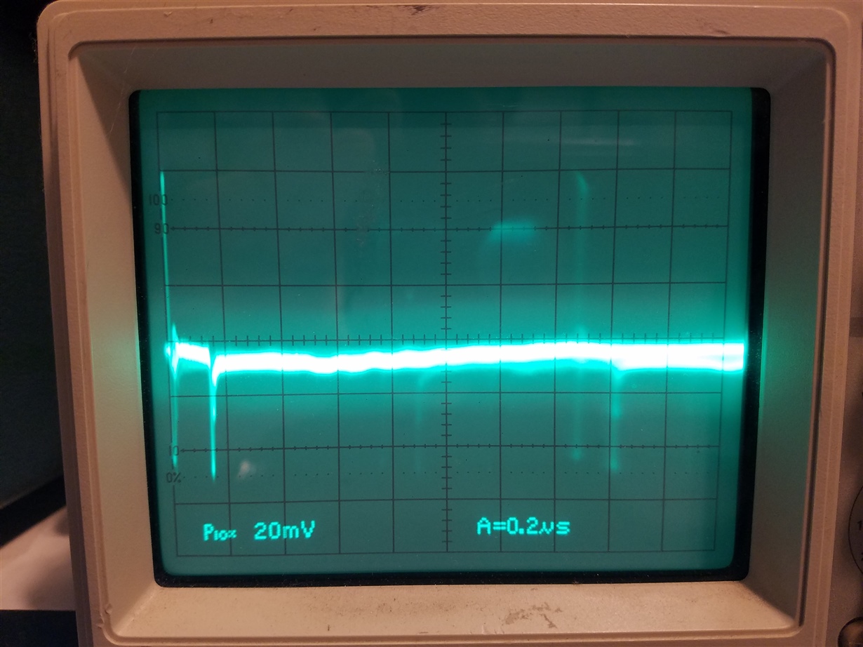
    With respect to the scope traces.  I pulled-out an old 100MHz analog scope to look at both the AC and DC components (with and without 20MHz filtering) to see what I might trigger on.  Here's the -4.5V Vout signal...

    Here is the GND signal (right on the output capacitor)...

    And here is the 12V signal being applied to the input of the DC-DC converter.  (NOTE, ALL SCOPE TRACES ARE AC-COUPLED WITH FULL 100MHZ BANDWIDTH, 8pF probe, 20mV/DIV and 0.2uS/DIV)

    I'll continue my test without the ferrite bead.  I'll be curious if you have some thoughts on that.

    Thanks, again, for your help in looking at this.  Tom.

  • Oops...sorry, my 12V and GND pictures are swapped....
  • Hi Tom,

    Do you have any updates on your test with the ferrite bead removed? Looking at your scope shots it looks like the spike on the 12V input voltage line is roughly +/- 60mV (assume you said 12V and GND pictures are swapped). The GND scope shows the reference node to have roughly +/- 20mV of noise. I don't think this is enough to cause noise issues into the switching converter.

    Do you have an E-Load you can connect this to and see if it still works?

    Regards,
    Jimmy
  • I'm not confident that I resolved this yet, but without the bead, I have not blown up any more parts and I have been running for days.  During by board clean-up here, I'll get myself some more headroom on this specification.  I'm confident that this is the issue.  Thanks so much for your help on this.  Tom.