This thread has been locked.

If you have a related question, please click the "Ask a related question" button in the top right corner. The newly created question will be automatically linked to this question.

TPS63060: Vout not consistent

Part Number: TPS63060

Hi,

    We are using TPS63060 to maintain a switched power supply of 5.0VDC for our embedded modem that is on the main board.

Source of power for TPS63060 and main board: 4 x D cell ( alkaline)=6.1 VDC

Power requirement for modem when powered ON: averages about 175mA @ 5VDC  and peaks to 300mA at transmit, we need the modem ON for 10 seconds or so to transmit and is turned OFF totally after , via the EN enable/disable on TPS6360. 

   We have about 10 PCB that we have fabricated per the layout and schematics shown below ( with 4 fingers on each side on the belly/thermal pad). Each board is exhibiting a different Vout characteristics for the TPS63060. For initial testing we have EN for TPS63060 always high/enables and not toggling EN to create switched output from TPS63060 ( EN of TPS63060 is set high by the PIC18F4620 micro controller on the main board).

a. Some boards have initial Vout of 5.1VDC (with minimal load of 1-3 MOhm resistor), but with the modem as load, Vout does a nose dive and Vout drops to about 2VDC, the modem powers off at around 3.5 VDC and hence no load but Vout never rebounds back.

b. On some of the other boards from the same lot Vout maintains 5.1VDC with the modem present as load, but only on the second power cycle,  in other words: power on main boards from D cells, main board working but Vout of TPS=0 to 0.2VDC. Reboot the power and it works the second time and maintains 5.0VDC. After the second power cycle EN on/off consistently gives desired Vout. But why the need for second power cycle?? Its almost like some of the caps needs to get some charge built up, so with the charge built up present on the second power cycle it works. If I power off the board for a few minutes and retry same problem ....needs a power cycle. But if I retry within few seconds it does not need the second power cycle

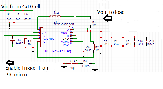
Figure 1: Schematics

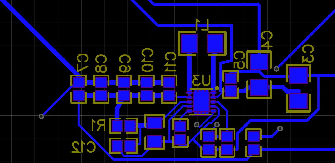
Figure 2: Partial PCB layout of the TPS63060 components only.

Please advise!


  • Hello DD,
    from the layout picture i cannot tell whether the PowerPad is correctly connected to GND. I don't see vias that connect it to a different layer.

    Could you share your gerber files (or similar)? -> you can send it to lbs_request@list.ti.com with the thread topic as subject.

    regards,
    Julian
  • Also, here is the component list/manufacturers part number for the parts shown above, should there be some concern:
    C3 & C4: 10uF, 25V 10% Ceramic Caps from Murata part # GRM31CR61E106KA12L
    C5, C11 & C6: 100nF, 50V 10% Ceramic Caps from Kemet part # C0603C104K5RACTU
    C7, C8, C9, & C10: 22uF, 6.3 V 20% AVX part# 06036D226MAT2A
    C12: 10pF, 25V 10% Ceramic Caps from Kemet part # C0603C100K3GACTU
    C13: 220pF 16VDC 5% Film Caps Panasonic part# ECH-U1C221JX5
    R1 , R2 & R4: 1MOhm, 0.5% .33W Thick Film Resistors from KOA part# SG73G1JTTD1004D
    R3: 111K Ohm 0.1 % 125mW Thin Film Ressitor from Vishay part# TNPW0603111KBEEA
    L1: 1uH, 10% Murata part# LQH31MN1R0K03L, then switched it with 1uH 20% from Coilcraft # XFL4020-102MEC to increase max DC current and reduce resistance
    U3: Switching Voltage Regulators 2.5-12Vin,2.25A Sw Crnt Limit, part #TPS63060DSCR
  • Julian,
    Email just sent with your requested items. Also, I have updated the parts list below.
    Thanks
    DDA
  • Hello DDA,

    thanks for the gerber files.
    It seems that the PGND/power pad is floating/not connected to GND. Can you confirm that?
    If that is the case it could explain the phenomenon that you describe. GND (pin7) and PGND do not have same potential in this case which causes the erroneous behavior. Please check the recommended layout in the datasheet. www.ti.com/.../layout

    also the Power and GND traces on the board are quite thin. Thicker traces or Planes/copper pours are recommended to lower the impedance.

    regards,
    Julian
  • Julian,
    Thanks for the update, do you have any additional concerns?
    Like spacing of component s or specification of any of the parts? I would hate to run another iteration of the PCB fabrication without being entirely sure that the issue will be likely resolved.
    Thanks
    Best ,
    DD
  • Hello DD,

    this is unfortunate, but you can definitely post here again for a layout review before PCB manufacturing.
    Unfortunately we don't have a layout guideline for buck-boost devices, but some point are covered here: www.ti.com/.../slva773.pdf

    The specification of the surrounding components looks good to me.

    You might be able to place the TPS63060 a bit more up on the footprint, such that you can solder a blue wire between Powerpad and board ground (close to the device). This is for sure not perfect but it can give you an estimate whether it works (light load should be ok).

    regards,
    Julian
  • Hello DD,

    I am closing this thread. Please post again if you have further questions.

    regards,
    Julian