This thread has been locked.

If you have a related question, please click the "Ask a related question" button in the top right corner. The newly created question will be automatically linked to this question.

BQ34Z651: systematic discharge FET failures killing products

Part Number: BQ34Z651
Other Parts Discussed in Thread: BQ40Z50

Hi There,

I have been having issues recently with discharge FETs failing in my battery packs, leading to free discharge of the pack. This causes many protection issues, especially the lack of under-voltage and over-current protection.

A schematic snippet of my design is as follows:

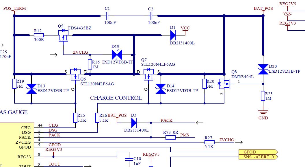
This design more or less follows the reference design with added TVS gate protection on all of the FETs

The FET I selected - for its low resistance - and in line with the design recommendations is this (data sheet):

https://www.st.com/content/ccc/resource/technical/document/datasheet/group3/75/d2/0c/9e/a7/af/4f/92/DM00161833/files/DM00161833.pdf/jcr:content/translations/en.DM00161833.pdf

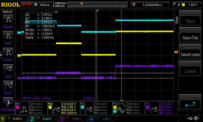
The death of the discharge FETs seems to be happening under usual operation conditions (not strenuous tests) and is only realized when the pack fully discharges and it fails to turn off (despite the gas gauge attempting to - as verified by scoping the DSG net). This issue seems to be limited to the discharge FET as I have not observed any issues with the others.

In addition to the protection shown in the schematic above the pack as a whole is protected with spark gaps and the following TVS diode.

http://www.vishay.com/docs/87649/tpc11cathrutpc36ca.pdf

 Does anyone have any insight as to what might be causing these issues / what I may have overlooked?

Thanks,

David

  • David, that portion of schematic looks OK to me. Are you saying the gauge sets XDSG and the fet still doesn't turn off?
  • Hi There,

    What I am saying is that the gas gauge sets XDSG and the voltage on the DSG net drops off as it should but the FET stays on.

    This can also be tested by asserting PFIN which turns off both the DSG and CHG FETs. in this case charging is prevented but discharging is still possible.

    When Q7 is replaced the pack functions normally.

    Thanks,

    David
  • Hi David,
    I have not seen ESD structures between the Gate and Source of the FETs in this configuration.
    I am not sure exactly what they would do, but can you try without these ESD Devices? (D13 and D14)
    Regards,
    Swami
  • Hi Swami,

    A previous iteration of this battery controller did not have these ESD suppression diodes and were were seeing occasional failures of all the power FETs involved in the circuit. Adding these TVS diodes has eradicated the failures of every FET except the DCHG FET. The addition of these diodes seems to be in light with best practice according to the literature

    As such I am reluctant to take them off again.

    Thanks,

    David

  • What is the purpose of D3? Please remove it and short across it. See if it works.
  • Hi There,

    In my application the battery pack needs to be able to wake up for the first time (out of shutdown) without the requisite charger input. So there is a switch that feeds POS_TERM into PACK to wake the gas gauge up. D3 is there to prevent this wakeup voltage/current from reaching the BAT_POT terminals on the pack which would in turn power downstream devices.

    As such removing D3 could be problematic, so I must ask, what is your justification for removing D3? What problem is it likely to be causing?

    Thanks,
    David
  • To clarify, my wakeup switching is more or less analogous to the push button S1 in the reference design for the bq40z50 which can be seen on page 17 of the following pdf. The difference is that I am using the diode D3 to prevent current flowing through to the pack output during this event.
  • Our IC design doesn't support it, With a diode, the DSG pin will be driven to our Pack pin which can no longer follow the external Pack voltage and will likely not allow DSG to turn-off.
  • Hi There,

    It makes sense to me that you would be driving to PACK, what I have observed is that the gas gauge does a perfectly fine job of turning off the DSG FET. Vgs is usually at about 200mV. If DSG is being driven to PACK which, due to the diode is artificially lower than the true value, I would expect it to actually do a better job of turning off the FET as Vgs would be even lower than the usual value. Is there an error in my logic here?

    If D3 was to be replaced with a resistor (as per the reference design) how large can that resistor get without issues? The data sheet only specifies a current draw during startup (1uA) which would suggest I can make the resistance 10K Ohms with only a 10mV drop, which is fine by me. Are there other current draws that I should be aware of?

    Cheers,

    David
  • Yeah, 10k on the pack should do. I can't think of anything else that would result in a large current. If it doesn't pan out, you can try a 5k.
  • Hi There,

    I will certainly do that to see if it makes a difference. But I still don't see how this could be related to the FET being damaged.
    I concede that I did deviate from the reference design but I doubt that puts the FET at risk.

    Cheers,

    David
  • Additionally, I would expect the CHG FET to get driven to BAT when it is turned off is that correct? BAT is sourced from POS_TERM through a diode exactly as I have with PACK. So that begs two questions, why are these supplies different in the reference design, and why is it apparently an issue with PACK but not BAT?
  • The IC handles the two pins very differently by design, it's got to do with the power controller.
  • Hi There,

    Thanks for that clarification, can you also address my question as to how the diode would change the FET drive such that it would damage the FET?

    Cheers,
  • Expect to hear from me later next week (7 days). I have to check a few things with design on this. I just know that this is not recommended and will kill the FET.
  • Hi There,

    I just wanted to share this attached oscilloscope screen capture with you to see if you any light on what is going on.

    This show the Gate voltage of the DSG FET in yellow, the Soucre Voltage of the DSG FET (Battery Pack output) in blue and calculated VGS of the FET in purple. This image is captured on the first startup of the device. 

    The device is woken up with a 1s pulse on PACK and in response to this pulse the gas gauge is partially turning on the DSG FET Vgs = ~2,2V. This partial turn on could in the presence of a multiple amp load cause the FET to burn up. 

    Can you explain why the gas gauge is doing this? And how I can stop it doing so?

    Thanks,

    David

  • For the DSG FET to be off the gate has to follow PACK. If it can’t, the FET isn’t guaranteed to be off. Therefore, it might be on but also could with a lower gate drive than intended. With a higher resistance channel, the power dissipated in the FET can be much higher than normal if the system tries to draw current in this semi-off condition. The FET damage can accumulate over time since the turn off will happen slower than intended.

    So, please do not deviate from our reference design.
  • Hi There,

    I will certainly remove the diode to be more like the reference design. But I am not sure I am seeing the symptoms that you are referring to. In the scope capture I send above you will see that DSG has no problem tracking PACK to a sufficient level to keep the FET properly off. It seems that the issue is that it decides not to do that sometimes, for example during the startup pulse pictured the FET is being poorly high-side driven so the device is clearly trying to turn it on but is doing a bad job of it. Is there a way this pulse on startup can be avoided?

    Thanks,

    David

  • I'm sorry but the drive is what it is. If we filter it, then we may delay the FET switching time.