


Dear,
our client use LM5116, power spec and schematic as below, and we find IC have damage risk.
sysem power spec:
• Input Range: 72V to 100V
• Output Voltage: 12V
• Output Current: 2A
schematic:

damage picture:
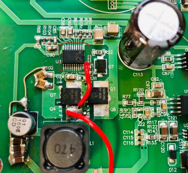
measurment pin to GND.
|
LM5116 Fail IC |
||
|
|
Pass |
Fail |
|
PIN |
to GND Ω |
|
|
1 |
3.35M |
x |
|
2 |
3.93M |
4M |
|
3 |
4.16M |
11 |
|
4 |
3.82M |
3.86M |
|
5 |
3M |
3M |
|
6 |
GND |
GND |
|
7 |
3.8M |
3.8M |
|
8 |
4M |
4M |
|
9 |
3.27M |
3.3M |
|
10 |
3.8M |
3.9M |
|
11 |
4.06M |
4.12M |
|
12 |
4.4M |
4.47M |
|
13 |
2.2 |
4.31 |
|
14 |
GND |
GND |
|
15 |
3.7M |
4.53 |
|
16 |
27K |
29 |
|
17 |
84K |
62K |
|
18 |
3.27M |
12K |
|
19 |
10M |
15 |
|
20 |
4.7M |
10 |
measurement waveform:

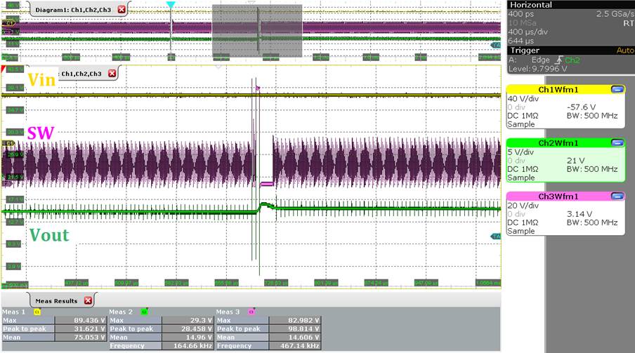
Also we use AN-1596 LM5116 Evaluation Board to change output voltage 15v, but we find IC Temp Tc was pretty high.

If any suggestion, Please advise me.
Thanks,
Best regards,
Lawrence.

