This thread has been locked.

If you have a related question, please click the "Ask a related question" button in the top right corner. The newly created question will be automatically linked to this question.

TPS2549: About TPS2549 communication and USB battery charging specification

Part Number: TPS2549

Hello.


There is a system that uses TPS 2549 in the project currently in charge.

I verified the designed completed board, but this IC will behave unexpectedly.

The purpose of use and the system configuration diagram of this IC are shown below, so please tell me which part is the problem.

·Purpose

1) This system communicates while charging the Android tablet. However, the tablet side functions as an OTG host device.

2) TPS 2549 complies with BC specification. I also decided that TPS 2549 also corresponds to the ACA (accessory charge adapter) specified in the BC specification.

    It is intended to communicate the tablet as a host device using ACA and let the tablet supply 5 V / 1A of electric power.

· Diagram

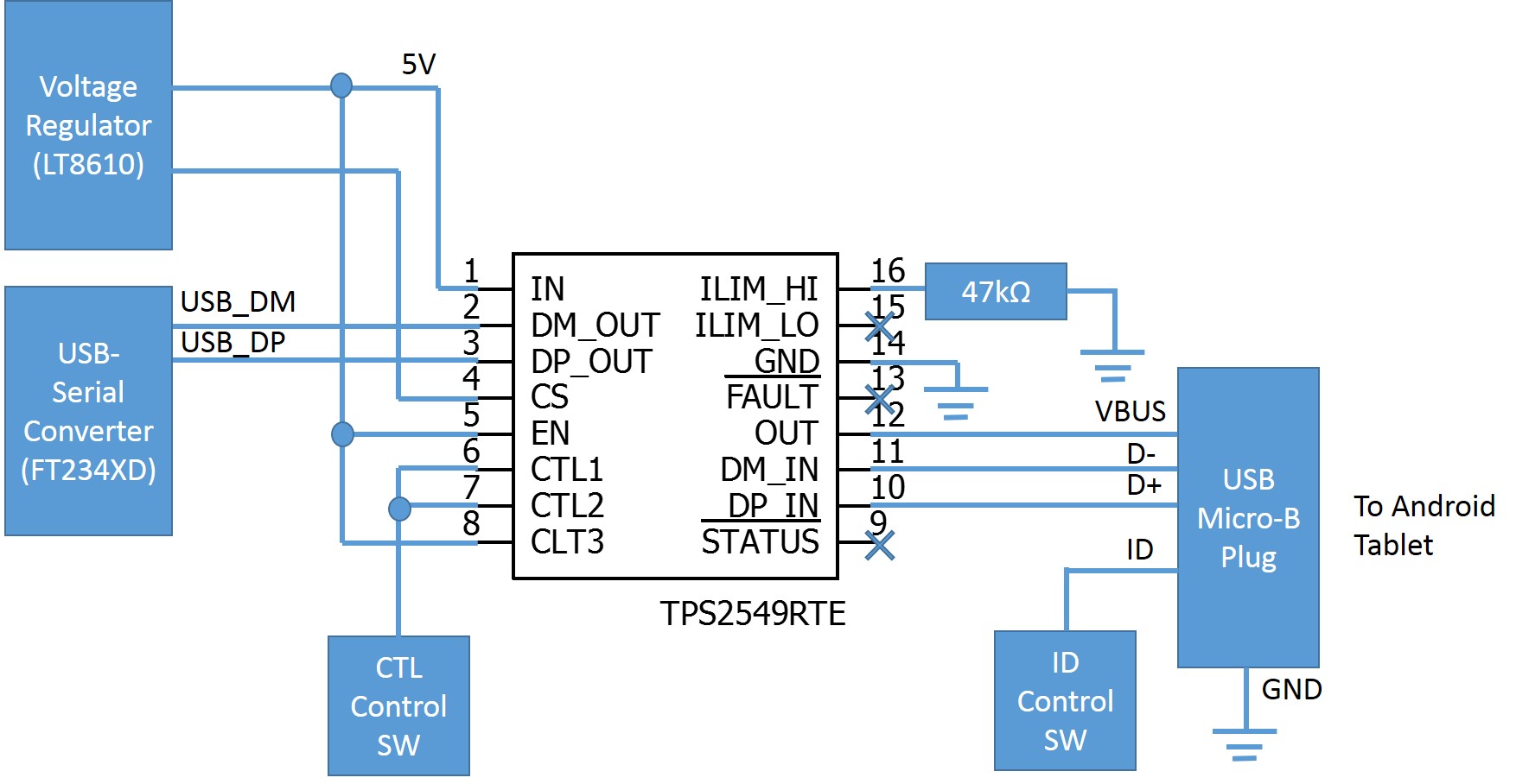
1) IN / OUT of the 5V line and current limit were functioning normally.

2) Only CTL 1 and CTL 2 can be switched to HIGH / LOW for CTL control SW.

    Since these are connected by a circuit, only (CTL 1, CTL 2) = (HIGH, HIGH) or (LOW, LOW) can be selected.

3) According to the OTG standard, the ID control SW can select whether to short the USB ID terminal to GND or 124 kΩ to ACA detection mode.

4) DM_OUT and DP_OUT are connected to FT 234 XD of FTDI.

    We are planning to communicate with each other on a device connected downstream of the Android tablet and FT 234 XD.

· Problems and questions

1) The above 4) can not be done. Specifically, when this system is turned on, the voltage regulator is activated and 5 V 1A is supplied to the tablet, but communication is not established.

    Is there a problem with USB detection?

2) Does TPS 2549 support OTG? If so, what is the correct behavior?

3) Because we are developing for the first time using USB, we do not fully understand the USB specification.

    Please tell me the contents of the USB specification if there is a problem.

Thanks.

  • · Problems and questions

    1) The above 4) can not be done. Specifically, when this system is turned on, the voltage regulator is activated and 5 V 1A is supplied to the tablet, but communication is not established.

    Is there a problem with USB detection?

    The TPS2549 can act as a DCP, which requires it to be able to act autonomously to provide power at the designated level without making a connection. If you configure the part as a CDP, then you will be able to provide 1.5A of current and maintain a data connection.

    2) Does TPS 2549 support OTG? If so, what is the correct behavior?

    The TPS2549 does not directly support OTG. If you want to support OTG, you will have to add in additional circuitry that will disable the TPS2549 upon power up, perform the OTG connection detection, provide the input power path if OTG is enabled. If this circuitry can control the enable port of the TPS2549 to disable the part when you are in the power input mode of OTG, then the TPS2549 can be used as part of the ssytem

    3) Because we are developing for the first time using USB, we do not fully understand the USB specification.

    Please tell me the contents of the USB specification if there is a problem.

    If you plan to support OTG, then you will have to design you power system to fully support the USB OTG spec and the BC1.2 specification if you want to support more that 5V/1A current levels.

    I am not able to provide you with a full set of parts to make a USB solution because I am not familiar with the entire power part library at TI.

    Regards,
    Chuck
  • Dear Chuck.
    Hello.

    Thank you for quick response.

    > If you plan to support OTG spec and the BC1.2 design if you want to support more that 5V / 1A current levels.

    I have an additional question.
    1) In the USB standard, when OTG is permitted, the tablet becomes a host. Is the connection direction of TPS 2549 and tablet correct on the IN side as shown in the configuration diagram?

    2) Will OTG certification be performed before or after certification of BC standard?

    3) When is TPS 2549 mode switching applied? I will list candidates below.
    · When TPS2549 power supply is input.
    · When EN pin of TPS2549 is set to HIGH.
    · When output USB is connected.
    ·other

    4) What kind of functions does ClientMode have specifically in the CTL mode? Also, what is the signal of D + / D - when connecting the tablet in this mode?

    Thank you.
  • 1. The TPS2549 must be placed in client mode when the device is in OTG device mode. This has to be done because the power path must be disabled.

    2. OTG has to be determined before BC1.2

    3. Mode switching will occur on any change to the CTRL pins. It will also update when EN or Exit of UVLO (Under Voltage Lockout) on the first powerup.

    4. The Client mode specifically disables all power path functions, but ensures that the datapath is enabled. This mode allows the D+/D- path to function with input power applied to the port.