This thread has been locked.

If you have a related question, please click the "Ask a related question" button in the top right corner. The newly created question will be automatically linked to this question.

TPS40170: Failed EMC test

Part Number: TPS40170
Other Parts Discussed in Thread: LM5146-Q1

Hello everybody,

Our product using TPS40170 failed on EMC radiated test at ~96MHz - so it's definitely common-mode noise problem! We narrowed it down with EMC probes and Spectrum Analyzer and we think the problem lies in buck.
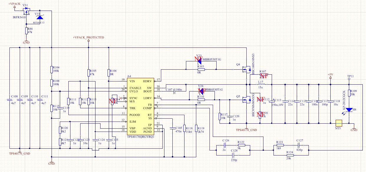
My schematic is:

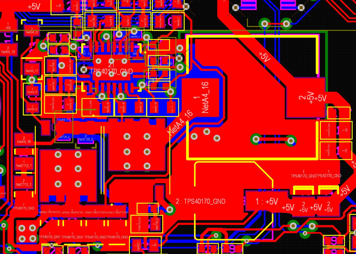
During PCB layout I paid attention for "power" loop to keep it small as possible. Layout looks like:

I did measurements on some critical points of the system: SW, LDRV, HDRV, OUTPUT node using "short ground probe". 

HDRV node:

LDRV node:

SW node:

Output 5V:

Of course, one of the possible solution is to add common-mode clamp on the input, but I would like to mitigate the source as much as I can.

  • Hello tuv0k,

    I am forwarding your inquiry to our controller expert, Tim.

    Regards, Robert
  • Hi tuv0k,

    Your waveforms look relatively clean. Depending on the frequency at which the failure related to radiated emissions occurs, here are some general recommendations:

    1. Use a common-mode choke in the input EMI filter (see LM5146-Q1 EVM user's guide for a suitable part number from TDK).
    2. Remove SW vias under the low-side FET drain as they couple noise to the bottom side of the PCB.
    3. Connect a 10nF-100nF cap very close to VIN and GND temrinals of the MOSFETs. This cap provides high-frequency decoupling and redcues the effective switching loop area, thus minimizing magnetic field coupling.
    4. Ensure they is a full GND plane on layer 2 as close as possible to the top layer (e.g. 6 mil spacing).

    Please see this link for a series of EMI articles, in particular part 6: www.how2power.com/.../EMI_Guide.php

    PS: you can remove the 10nF cap and 10k resistor on the low-side FET gate.

    Regards,
    Tim
  • Hi Timothy,

    First I would like to thank you for trying to help me in this situation. 

    1.) Almost certainly. I would like to avoid this and use it as a last chance to dump radiation!

    2.) Understand you, but this would require PCB re-layout. It will be done on next batch! However, in that case L_FET would be hotter!

    3.) Tried without any changes!

    4.)It is. Spacing is ~0.125mm due to impedance control on other part of PCB

    I measured SW node and zoomed o-scope on the rising edge and saw a overshoot with frequency ~165MHz(We were above radiation limit on that frequency as well). Afterwards, snubber did not help and it's not a feasible solution due to the fact that device is being powered up using custom made li-ion battery so input voltage is not fixed. 

    I went for adding 10R resistor in series with HDRV FET gate. That helped a lot. Overshoot is fairly visible at the moment, and common-mode radiation measured using current clamp and spectrum analyzer is -6dB at least.

    We got time slot in radiation chamber next Monday - will get back to you with results!

    p.s. 10nF could be removed, but 10k could not because it sets SCP/OCP limit!

    Thank you for your help!

    P.

  • Hello,


    We had not heard back from you regarding results. We will assume that the issue is resolved? if not, please feel free to reopen thread.

    Thank you.

    David.
  • We passed successfully by adding 10R in series wih High Mosfet. In future PCB variant we will remove vias under SW node to minimize noise coupling.

    Thank you for your support and best regards!

    P.