This thread has been locked.

If you have a related question, please click the "Ask a related question" button in the top right corner. The newly created question will be automatically linked to this question.

TPS7A63-Q1: TPS7A63-Q1 ESD Sensitive & pcb Layout problem

Part Number: TPS7A63-Q1

Dear TI:

   Custom use tps7a6350-q1 for ESD Test, But it fauiled ----nReset pin output low voltage.and external light blink one time.
the output cap is 10uf*3=30uf.  I Double may the bad PCB layout cause the problem.

the test condition: 
ESD Voltage : 2kv /4kv ...
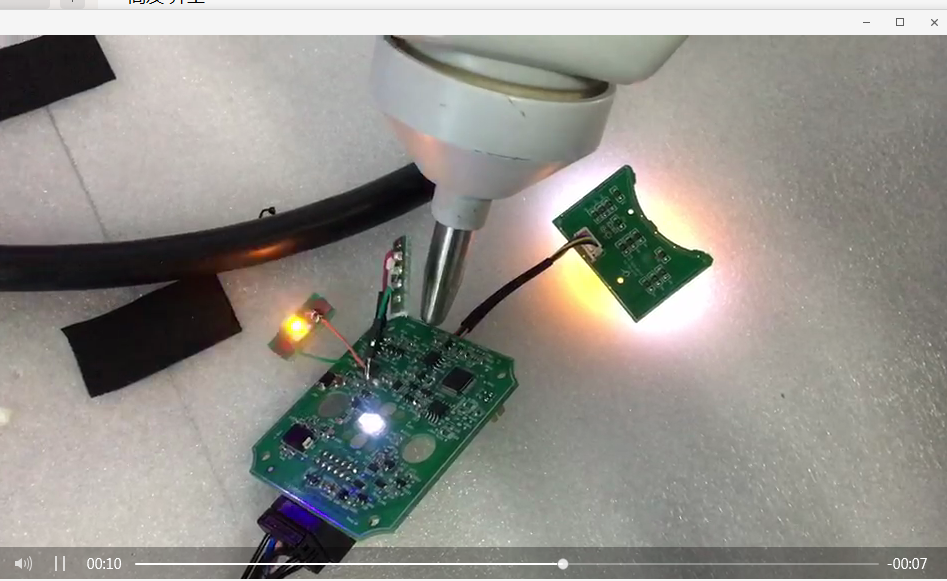
  

I Double the interruption from the nReset net.  Cause the 5v  output voltage (white led) has no blink.


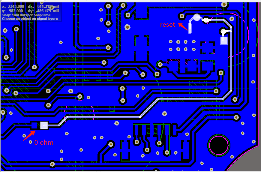
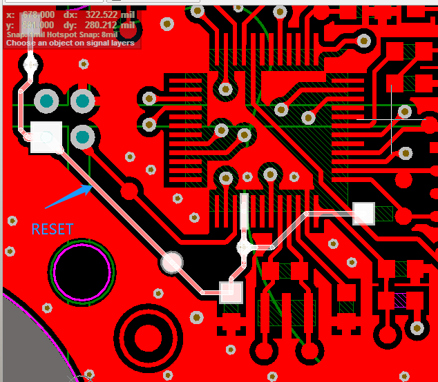
Pcb Layout as fellow:

  • Hi ,

    We rate our devices per the AEC Q100-002 standard.  TPS7A63-Q1 is rated to the HBM ESD Classification Level H2 with a 4 kV HBM.

    Please ensure that you follow the test procedure as specified by the Automotive Electronics Council:


    Very Respectfully,

    Ryan

  • Hi ,

    Since it has been a week without a reply, I assume that this thread is resolved. If this is not correct, please feel free to post again.

    Very Respectfully,
    Ryan
  • Dear TI:

    Sorry ,Update so late. the abnormal  phenomena still exist. ESD Test condition:  Voltage:4kv   Interval:1s . Mode:IEC LEVEL1

    1. When i do ESD Test, the nReset pin will be output low voltage , so i cutoff the nReset  network nearby, and add a little pcb indicate with a led. But the situation still same.
    2. I guess may the bad pcd cause the problem.  -----  Large power  disturb the 5V network , dropdown to the threshold value, lead to the nReset pin  output low voltage.
    May i know how to verify the result or there's other reason can cause the problem. 
    thanks 

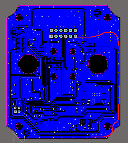
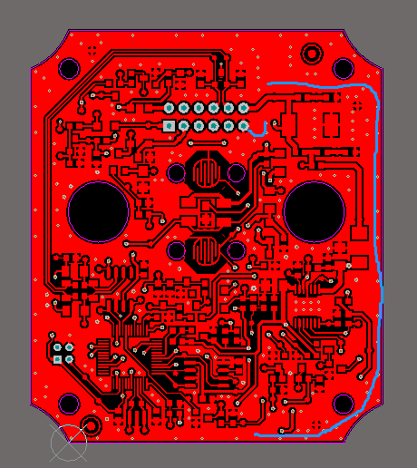
    the PCB Layout:

  • Hi ,

    Could you give us a better understanding of the failure symptoms? If you power cycle your board, does the part operate as normal?

    The path that you mark appears to be long and narrow. As such we would expect there to be an inductive element that will increase the current flowing through the path. Do you have a way to reduce the inductance on this path? For example if you add a capacitor to counteract the inductance local to the LDO pin, do you see the same result?

    Very Respectfully,
    Ryan
  • Dear Ryan:

    More information:

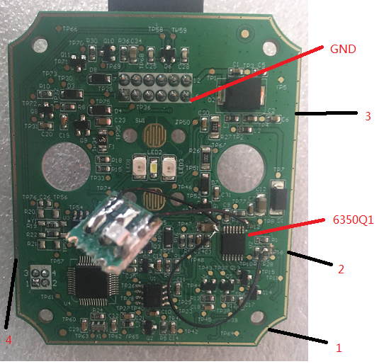
    The surface of the customer's casing is 25KV static, customer confirmed static electricity caused TPS7A6350Q1 reset. Considering the arc, the 4KV static simulation test is currently performed on the circuit board.


    PCB:

    Static electricity 1# 2# is particularly easy to result in reset, 3# is also easier to reset, but 4# is not found to result in reset phenomenon.

    Debugging steps: 

    1. It is suspected that nReset been interfered. By cutting the line, disconnecting the external circuit, and comparing the two ends with a small light board, the phenomenon still exists.

    2. At the copper foil, directly connect the jumper to GND, the phenomenon has not been lifted.

    3. From the Datasheet, reset will only result in 5v output voltage drop. Disconnect the 5v network in the sensitive area, the phenomenon still exists.

    May i know the reason is GND Network interfered or not?    copper (Out ring) use single point ground is suitable?
    thanks a lot.


  • Hi ,

    Please provide a schematic of your application local to the LDO showing your input voltage, output voltage (5 V), and the components on each pin for the LDO.

    Please also provide the output voltage of the LDO at the time that nRST is logic low.

    Very Respectfully,
    Ryan