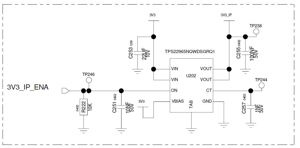
We are using two load switches TPS22965NQWDSGRQ1(U202) and TPS22965QWDSGRQ1 (U203) in our design.
Please refer the attached images (Sch1 and Sch2) for design reference.
Design Details :
| Parameters | U202 | U203 |
| Input Voltage | 3.3V | 1.8V |
| Bias Voltage | 5V | 5V |
| Enable signal | Controlled by uC (3.3V LVCMOS level) | Controlled by uC (3.3V LVCMOS level) |
| CT voltage (probed after fault) | 0V | 0V |
| Output Voltage (probed after fault) | 0V | 0V |
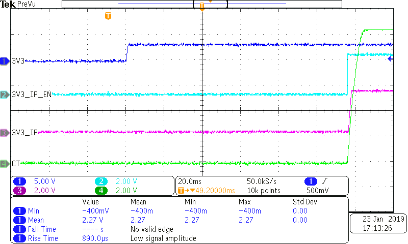
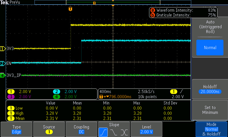
Problem observed :
Load switch outputs are not raised as we expected even though the input voltage, Enable signals are driven properly.
Things noted:
CT voltage is not appeared on the CT capacitor pin.
Suspected that load switch is not able to generate the gate voltage, hence output voltage is not appeared at the output.
Clarification / Support required:
Causes which will failure the load switch.