This thread has been locked.

If you have a related question, please click the "Ask a related question" button in the top right corner. The newly created question will be automatically linked to this question.

UCC28711: TIDU412A Power Supply Design Issue

Part Number: UCC28711
Other Parts Discussed in Thread: AMC1301, TIDA-01541

I am designing a power supply for a variable frequency drive by following the design of TIDU412A. The power supply gets input DC voltage from the main vfd rectifier; I have excluded the diode rectifier at the input of the power supply and my power supply design starts from L1 and L2 inductors of schematic 8.1 and follows the rest of the design as detailed in TIDU412A.

I am checking the voltage at connector j=J5 coming from vdc_meas in 8.1.It should reflect the input dc voltage(divided by turns ratio and through the resistive divider) but this result is not consistent when I change the input dc voltage. 

Kindly help me out with this.

The schematics(PAGE 31) and design are with reference to TIDU412A:-

www.ti.com/.../tidu412a.pdf

  • Hi Ahsan,

    Thanks for your interest in TIDU412A. What is the voltage you see at J5? Does the voltage change with input? Does the -16V output voltage remain regulated as you change the input voltage? Do you see the duty cycle of the flyback change as you change the input voltage? Does the behavior change if you apply load to the +16V and -16V rail?

    Best Regards,
    Ben Lough
  • Hi,

    I have attached a table of values that I measure at J5 with different input voltages. There is no load on the -16V output as I am not using the -16V voltage so I have not connected D27 and D25 and the subsequent components for 16V and -16V. 

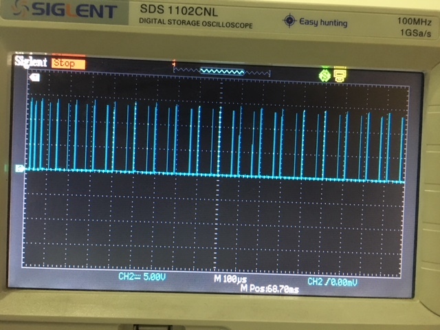
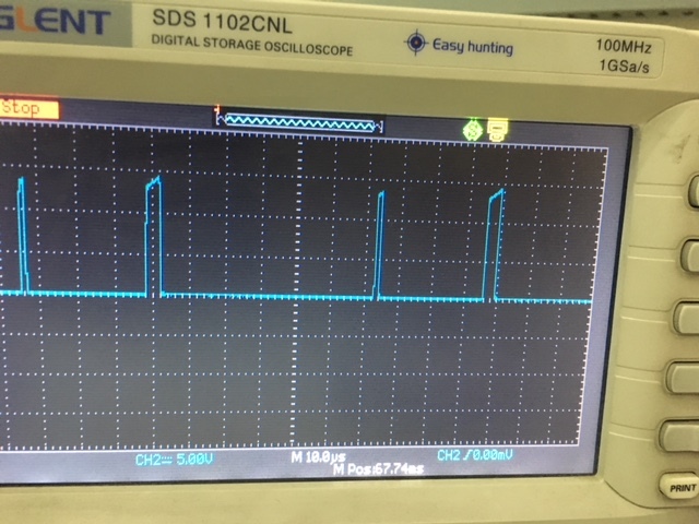
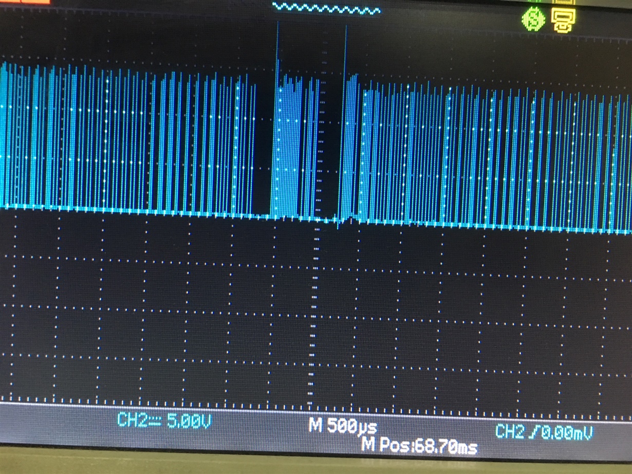
    The switching frequency (as measured at pin 6 DRV of the switcher) alternates between approx 30kHz and 60-70kHz and the duty cycle stays between 6 to 8 %. I have verified this result at different input voltages.

    I am attaching the gate signals oscilloscope screenshots for your reference.


  • Hi Ahsan,

    The duty cycles seems small. In this design, the DC link voltage measurement is dependent on the MOSFET ON time in order to sense the DC link. Do you have any load on the 24V output? Could you try applying 2A load on the 24V rail and see if the voltage at J5 increases?

    Best Regards,
    Ben Lough
  • Hi Ben,

    Initially I was drawing just a few hundred milliamps, I have now increased it to 1.3A. The voltage at J5 does change a little bit. For example, at 430Vdc input, the voltage at J5 was 1.632V initially, which changed to 1.86V with output current 1.3A. But it is still not the voltage that should be seen at J5 as per equation 54, page 22 of TIDU412A.  

    The duty cycle also changes a little bit. The on-time remains around 5us while the frequency alternates between 35 and 71kHz, resulting in duty cycle in the range of 17 to 35%.

  • Hi Ahsan,

    Apologies for the delayed response. The reason for the lower than expected voltage at J5 is likely because of the changing frequency and duty cycle at steady state. At 2A load on the 24V rail, does the flyback have a consistent switching frequency? Perhaps the disconnected outputs is causing some oscillation in the bias winding voltage which is making the operating point of the flyback move around.

    Best Regards,
    Ben Lough
  • Hello,

    I have conducted various experiments with different loads on the power supply. One thing that I noticed was that the duty cycle does not stay constant if I connect load to the Vaux supply (Vaux was previously loaded all through our previous discussions). So I disconnected the Vaux load (the duty cycle stopped varying) and observed the J5 voltage at different loads. The result is that the voltage at J5 is dependent on the the input dc voltage and the load connected to the 24V supply i.e. the ratio of input dc voltage to output voltage at J5 changes with change in input dc voltage as well the change in load connected to the 24V output. Whereas this ratio should stay constant according to TIDU412A. I checked this by loading and unloading the +/-16V output supply.

    Another thing which seems odd about the power supply and might be related to this issue is that if I connect inductors L1 and L2 as shown in schematic 8.1 of TIDU412A, the power supply operation becomes unstable, it stops working and starts generating pulses as if trying to turn on. This happens mostly at input dc high voltages at around 600V. But when I replace L1 with a diode it works perfectly fine. The dc input voltage that I am providing to the power supply bulk capacitors is coming from 1700uF VFD DC-Link.     

  • Hi Ahsan,

    Thank you for the update. I would expect some change in the voltage at J5 depending on the duty cycle. TIDU412 is correct when stating that the voltage at VD_MEAS will be the input voltage reflected by the turns ratio of the transformer. It is important to note that this is only true when the primary side MOSFET is on. When the primary FET is off D24 will be reverse biased. VDC_MEAS is then fed into an RC filter which will give you an "average" of VDC_MEAS and the voltage at J5 is the stepped down voltage from this average value of VDC_MEAS. If the duty cycle is large, I would expect the voltage at J5 to be larger. If the duty cycle is small, I would expect the voltage at J5 to be smaller.

    During your testing with L1 and L2 connected, was the DC input being applied to J2 in your test or is it being applied to J1?

    Best Regards,
    Ben Lough
  • Hi Ahsan,

    Just wanted to check how your debug efforts were going. Please let me know if there's anything else I can do to assist.

    Best Regards,
    Ben Lough
  • Hi Ben,

    The current sense resistor R22 is 0.91 ohm as mentioned in the handout. I had previously been using 1 ohm and I changed it to 0.91 ohm now and repeated all the tests. 

    But it is giving the same result. Increasing the load as well as applying the load at the Vaux changes the voltage seen at J5, plus the input to output voltage ratio also varies (with change in input voltage). I intend to use this voltage sensing to trigger an over/under voltage fault, but since there are too many variables involved which change the voltage at J5, I am afraid it will lead to faulty triggering.  

  • Hi Ahsan,

    I have asked the original designer of this reference design to comment on this.

    Best Regards,
    Ben Lough
  • Hi Ahsan,

    The original designer is out of office right now but should be back sometime next week. Apologies for the delay. If you would like other ideas for implementing input UVLO in your design I can suggest some alternatives.

    Best Regards,
    Ben Lough
  • Hi Ben,

    Any update?

  • Hi Ahsan,

    Apologies for the delayed response. With this indirect input voltage sensing method, any leakage in the transformer will impact the resulting voltage at J5. It is not a precise method for sensing the input voltage.

    If a more precise is needed, I would suggest using an alternative method. Other motor drive designs have used isolated amplifiers such as AMC1301 to implement input voltage sensing. For reference, take a look at page 3 of the TIDA-01541 schematic:www.ti.com/.../tidru21a.pdf

    Best Regards,
    Ben Lough