This thread has been locked.

If you have a related question, please click the "Ask a related question" button in the top right corner. The newly created question will be automatically linked to this question.

Reverse Current Protection using two PMOS in back to back configuration

Other Parts Discussed in Thread: LM74700-Q1, LM5060
  1. I have gone through TI's load switch options and couldn't find one that is rated for +50V and has reverse current protection. So I have to using discrete components to make a load switch.
  2. I am working on a circuit that needs reverse current protection. I have seen back to back mosfet configuration in a few of TI's app notes, and it seems to make sense. But after I built my PCB, after fully charged my capacitor, and then turned off the power supply, the current flowed right back to the power supply. Please check out my circuit below.
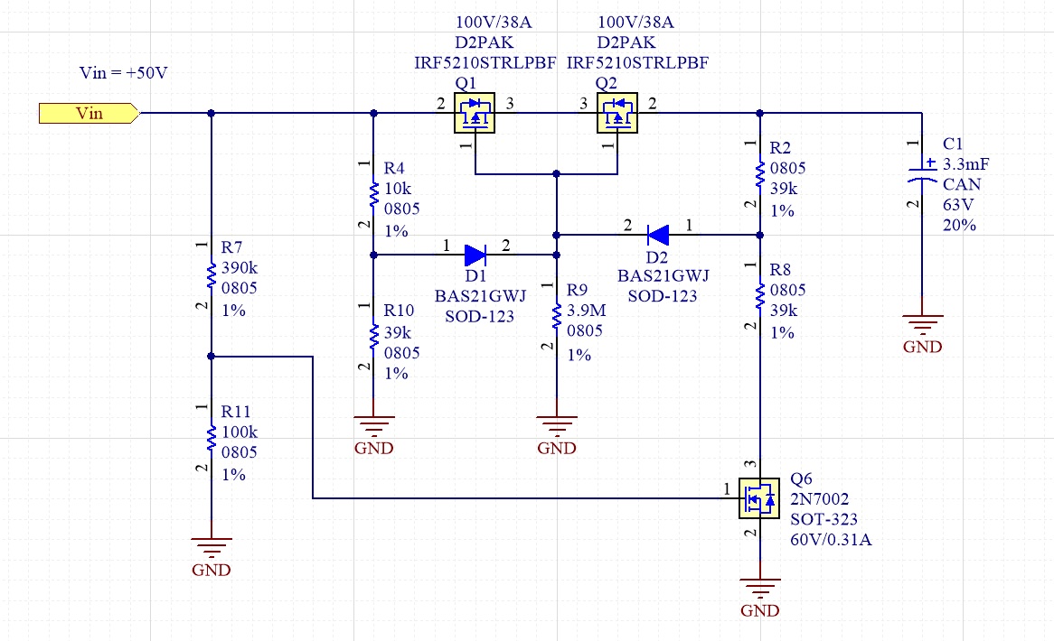
  3. Let me explain my circuit a little bit. Vin = +50V. I need to charge C1 and use it to run a pulsed (D=10%) circuit that requires every large current. I have a separate circuit that controls the max current to charge the capacitor, so that I do not need to worry about charging current for this circuit. During charging, my intention is to using R4 and R10 to keep Q1 and Q2 on when power supply is turned on; R2 and R8 sets up a node voltage that is always less than the gate voltage at Q1 and Q2 unless Q6 is turned off. When the power supply is on, R7 and R11 keep Q6 on. D2 blocks the current flowing to C1. Everything works on charging my capacitor. During discharging, when Power supply is turned off, R7 and R11 has no current flowing through and Q6 is off, and the gate voltage on Q1 and Q2 is pulled up to something like +49.5V while C1 has +50V, and Q1 and Q2 shuts off. Here is the problemQ1 and Q2 were never turned off. My theory is that any parasitic capacitance or slow power supply turn off action that can keep Q6 on for a very small mount of time, Q1 and Q2 will stay on, and current starts to flow back, and then most of the voltage on C1 appears at Vin and keeps Q6 for longer period of time. It creates a positive feedback loop and keep Q1 and Q2 on.
  4. I have done simulation and confirmed that the Q1 and Q2 are on after power supply is off.
  5. I would love to have some feedback from you guys because many of your load switches has reverse current protection. If you have different ideas on how to block the reverse current, I would love to hear them too. Using diode is not an option because forward current is too high, diode gets too big and consumes a lot of power.
  6. Thanks!

  • Hi Hong Pan,

    LM74700-Q1 is an ideal diode controller that can be used to drive N-Channel MOSFET to block reverse current for 50V application upto 65V maximum.

    Could you please let us know the current requirement for this charging application.

    If you require back-back configuration, LM5060 device needs to be added along with LM74700-Q1.

    Regards,
    Kari.
  • Hi Kari,

    On Charging, the forward current is 3A.
    All I care about is to block reverse current at this point. I do not care if I use one mosfet or two. Are you sure that I will not run into the same problem I have been having? I read through LM74700-Q1, and it seems very promising. Is it monitoring the voltage different between input and output, and decide to turn off the NMOS on if Vout-Vin > 11mV?

    Thanks,

    Hong
  • Hi Hong,

    Yes, LM74700-Q1 can block reverse current effectively and reduce the forward drop during normal operation close to 20mV.

    LM74700-Q1 monitors a IN-OUT using internal reverse current comparator and turns off the MOSFET quickly within 0.45us (typical, 1us maximum). Reverse comparator threshold is -11mV.
    LM74700-Q1 regulates the Vds (IN-OUT) to 20mV and this is done by an internal amplifier, continuously regulating the Vgs voltage of the MOSFET.
    This regulation helps to completely provide "Zero DC reverse current" using the internal amplifier and reverse comparator.

    Please note the -11mV threshold is used to calculate the transient reverse current (very short time of 0.45us).
    Maximum transient reverse current during a input short, would close to -11mV/ RdsON of MOSFET.
    DC reverse current is zero and this is a key feature of this device.

    This is much better than a diode, where lot of power is dissipated due to considerable forwward drop 600mV.

    Regards,
    Kari.
  • Hi Kari,

    Thanks for the explanation. It is very helpful. Here are a few more questions:

    1. Regarding the 20mV (Vin-Vout) voltage drop regulation for LM74700-Q1, if my power NMOS has Rds*Ids that is greater than 20mV, what is the behavior this controller when that happens? Do I have to pick a NMOS that has Rds*Operating current that is always less than 20mV? In the block diagram, it looks like if Rds*Ids is greater than 50mV, something is going to happen.

    2. On page 10 of LM74700-Q1 datasheet, it says "An internal charge pump is used to drive the external N-Channel MOSFET to a maximum gate drive voltage of approximately 15 V." is it saying it is going to drive the gate voltage to a maximum of 15V greater than the source voltage to reach 20mV (Vin-Vout) voltage drop regulation?

    3. Is there a reason why LM74700-Q1 cannot drive two back-to-back NMOS? Just curious because I cannot deduce this information from the datasheet. It looks like if I can use back-to-back configuration, the EN pin becomes really useful in some applications.

    4. When is this device ready for sale? It looks like only preproduction is available through TI store.

    Thanks a lot.

  • Hi Kari,

    Just thought of another question to ask:
    You mentioned that LM74700-Q1 detects -11mV between Vin and Vout using RdsOn*Reverse Current, what happens in the case of a small reverse current? In my situation, when my power supply is turned off, it is presenting itself as a 3kohms resistor, and the max reverse current is 18mA. If my NMOS has Rdson around 20mohms, the voltage drop is 360uV. Will LM74700-Q1 detect this small mount of reverse current and block it? Or will it use GM Amp to shut off the NMOS because of the +20mV regulation between input and output?

    Thanks.
  • Hi Hong,

    1. If the MOSFET chosen is such that it Ids * RdsON(lowest) >20mV, then LM74700-Q1 cannot regulate and it will go into full conduction mode mentioned in the datasheet. It is recommended to choose RdsON such that, 20mV/I_Load_Nominal < RdsON < 50mV/I_Load Nominal. If the Vds is greater than 50mV, MOSFET will go into full conduction --> Gate will be fully enhanced. Otherwise during normal operating condition, gate will always be regulated (Gate need not be fully enhanced) to maintain Vds 20mV. The regulation and reverse comparator in combination works to makes sure that there is no DC reverse current during an input short (or supply or battery failure). Refer to the attached waveform showing this.

    2. Yes Gate voltage is driven above the source voltage (same as anode pin or input). Vgs maximum is 15V.

    3. Yes LM74700 can not drive back to back MOSFET, because it turns off the MOSFET by making Vgs = 0V internally. One of the MOSFET which is in the direction to block reverse current will be turned as its Source is at anode and Vgs is 0V. However for the second MOSFET, Gate to drain is 0V. This mean second MOSFET can not turn off fully. Its Source will have voltage = Drain - Vth of MOSFET.

    4. Preproduction is available and regarding the release, we cannot share this information online. But what I can say, it will release very soon.

    5. Incase of the small reverse current: Lets assume the input power is disconnected or turned off very slowly (not input short failure). Now there will small reverse current that would try to flow from output to input. But the Vds regulation circuit is continuously trying to adjust the gate voltage depending on load current. I mean, for higher load currents gate voltage will be higher and for lower currents, gate voltage would be lower, just above Vth of MOSFET. Now when the input supply is disconnected or turned off slowly (lets say 1ms to 10ms scale), load current is going to slowly reduce and gate voltage is reduced to maintain 20mV. This eventually would bring the Vgs close to Vth, which means RdsON is very high and as the current starts to reverse it will turnoff -11mV/New_RdsON. So there would not be any reverse current flowing.

    However assume the case of quick or fast input failure, where input voltage goes to 0V very quickly, now the regulation circuit cannot react very quickly and a reverse current -11mV/Nominal_RdsON will flow before the reverse comparator turns it off within 0.45us (typically, 1us Maximum).


    Regards,
    Kari.
  • Thank you! Very informative and very helpful!
  • Hi

    If this has resolved your question, please click "this resolved my issue" button.

    Regards,
    Kari.