This thread has been locked.

If you have a related question, please click the "Ask a related question" button in the top right corner. The newly created question will be automatically linked to this question.

TPS62751: TPS62751: performance with output current >800 mA

Part Number: TPS62751
Other Parts Discussed in Thread: TPS62651, TPS62750, TPS61088, LM27762, TPS61041

Dear Ti support,

I am performing test with the TPS62751 Step-Down converter.

My requirement are:

- input voltage from USB-C (from a tablet): 5V (can go as low as 4V when drawing 1.2A)

- output voltage 3.7V

- output current target 1A.

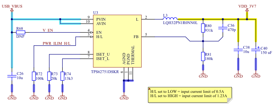
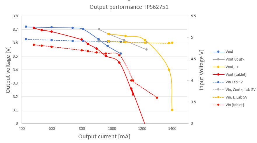
I performed my test on a dedicated layout (see schematic below), Rlim High is 20k which should limit the input current to ~1.23A. My observation is that the output voltage drops well before reaching the input current limit as shown on the graphic attached. Blue, Grey and Yellow curve are done with a lab 5V supply. Blue curve corresponds to the schematics, the Grey curve has an increase Cout (+ 3 cap ceramic X7R of 10uF), the Yellow has a increase inductor (3u3 with smaller R). This changes tends to improve the perforamance at higher load.

Then I powered the device with the tablet. The RED curve shows the performance with the tablet. The tablet voltage is reduced depending on the load (pink curve, right axis). and the ouptut voltage is not really regulated to 3V7 as we can see on the RED curve. (this measurement were done with the improved circuit , corresponding to the Yellow curve when powered with a regulated 5V input voltage).

Any recommendation to improve this circuit. I am hesitating to order the EVM to check if I get the same results, but maybe you can already inform me about some limitation of this circuit.

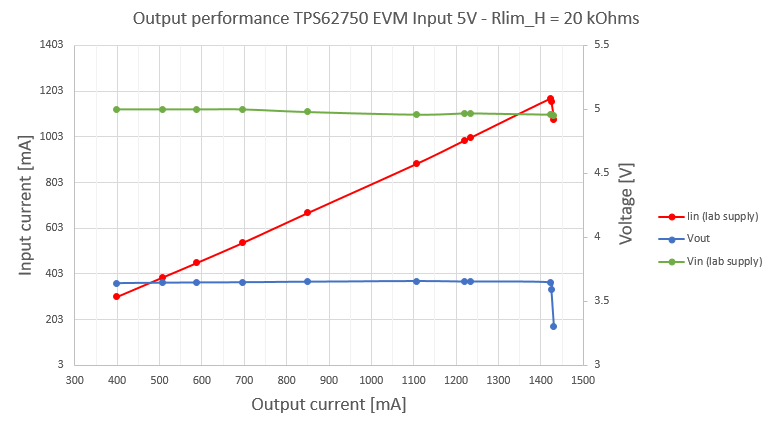
It seems that the datasheet figures are done with limitation near 700 mA (R_lim_U ~50kOhms), is this correct, I cannot find this information in the datasheet.

thanks for your help.

  • Hi Pierre,

    There are few things I would like to understand regarding your settings with your schematic and the expected behavior of the part. Is it the latest Schematic you are using here?

    I see R68 with a DNP comment, Is EN pin linked to VIN?
    You set the H/L pin to GND meaning the lower current limit threshold is set to 500 mA. I recommend you link it with the same resistor to VIN.
    I don't really understand what you mean by "The tablet voltage is reduced depending on the load (pink curve, right axis).". Can you rephrase it? Is the Tablet Voltage the input of your system?

    It is also recommended to place 10x150 uF poscap at the output of your system, Is it something you can manage to have?
    Thank you very much!

    Best Regards,

    Dorian
  • EN is asserted high  by a pushbutton controller (LTC2955) with a sufficient level and the H/L line are asserted high by the microcontroller. The configuration of those pins seems fine to me. 

    Yes^, the tablet voltage is the input of my system (but the plot shows also measurements done with lab power supply 5V), the voltage delivered by the tablet is load dependent as shown on the pink curve (I dont know if this follows USB spec, probably not, but I have to deal with it).

    I reorganize the curves, dashed ones are the input voltage of the TPS62751 (scale on right Y-axis).  Continuous line are Vout of the stepdown.

    As you can seen, increasing the Cout improve the performance. I can try to add more capcitors.

  • Hi Pierre,

    I think you meant that the dashed curves are the new Vout of your system when you added output capacitor, Am I right? Otherwise it looks like your Vout (continuous curves) hasn't changed, or it does not seem like it.

    The main challenge you are facing here and you understood it well, is that your tablet voltage input is limiting your system's performances. You will not be able to produce an output which will be better than your input.

    I encourage you to add capacitors like stated in the datasheet recommendations, 10x150uF poscap .

    Thank you.

    Regards,

    Dorian
  • Hello,

    thanks for your answer ! No, the dashed curve are the input of the system (connected to VIN of the TPS62651).

    Please only focused on the red curves (done with the tablet), I would expect a better regulation of the TPS62750 output voltage. For sure, the VIN falls as we draw more current, but input voltage is still above 4.5 V but the output falls too (well before the converter should start limiting the current). Is this normal ? -> I expect that the output is regulated at 3.7V until the converter starts to limit the current !

    Any comment welcome (but I will try to add this huge  capacitor network at the output !)

    Thanks in advance

  • Please note that the plot has two Y-axis, on the left for the output voltage, on the right, the input voltage.

  • Hi Pierre,

    Can you draw the same plots  but with your input current as X-axis? The current limit is at the input not output.

    If your system reaches the input current limit then no extra current will be allowed into your input. Meaning if the load at the output increases then your output voltage will drop.  

    I recommend you take a look at figures 7/8 of the TPS62751 datasheet, to have a better understanding.

    Thank you!

    Regards,

    Dorian

  • Hello Dorian,

    I understand that this IC limit the input current. However I am far from the limitation set by the Resistor. I will get my EVM and some tantal 1.5mF capacitor today. I will be able to compare and give you some better reference measurement.

    Something really not clear in the datasheet (I cannot find where it is stated) are the Resistor used as current limit High and Low, corresponding to all the Figure. It's probably something like 50k but could you confirm the used values ?

    thanks in advance

  • Hello Pierre,

    Good to know.

    This is indeed not stated, I added this a to TI’s change review process to modify this datasheet.
    The resistor values used for the figures are R3(Rlim_u)=49.9kOhm and R4(Rlim_l)=69.8k Ohm. Setting the lower limit at the 100 mA and the upper one at 500mA.

    Keep me informed on your progress.
    Thank you.

    Regards,

    Dorian
  • Hello Pierre,

    Any update from your side?

    Thank you!

    Regards,

    Dorian
  • Hello Dorian,

    For sure an update ! you will find attached some measurement done with the EVM and RlimH set to 20kOhms -> input current limit at 1.23A. I made test with 5V input and 4.5V input. Results are much better.

    Does the performance at 4.5V input match your expectation ?

    In fact, on the custom PCB, I have several DC/DC converter following the TPS62751 and in close proximity.

    1st stage -> TPS62751 feeding all 2nd stage power supplies ->

    2nd stage:

    - TPS61088 Boost converter to 10V

    - LM27762 Symmetrical supply with Charge pump and integrated LDO for Analog supply

    - TPS61041 Boost for High voltage with external switch (45V)

    When doing my test, I thought that all converter were disconnected, but I forgot to remove one 0Ohm jumper that feed the TPS61088 from the output of the TPS62751. Both switcher are very close to each other and the TPS61088 impacts the regulation of the TPS62751. Removing the 0Ohm jumper or adding a wire or a ferrite bead instead of this jumper solve the issue.

    It happen the same with the other boost TPS61041 when I reconnect the 0 Ohms jumper. (ferritebead solve the issue too).

    It is not clear what cause this. Maybe you have an idea, or know any guidelines from TI regarding multiple stage of DCDC converter design.

    At the end, if I replace the 0Ohms jumpers by a ferrite bead, it works and performance of the TPS62751 are as expected

  • Hello Pierre,

    Great, glad to hear that!

    I indeed would expect the 4.5V input to have a slightly deteriorated performance compared to 5V. The internal resistance of the high-side MOSFET (Rds_on) would increase because of less input voltage, creating higher losses which explain why at bigger currents you can observe that output performance changing.

    I don't really understand why this trick solve your issue, but i want to warn you that every compensation comes to a price. You need to be aware that using ferrite beads will modify your system transfer function resulting in possible oscillations. Your system could also be less responsive to transient response.

    "any guidelines from TI regarding multiple stage of DCDC converter design". I have not found anything yet, I thank you for this valuable feedback. We will definitely work on it!

    Thank you very much.

    Best Regards,

    Dorian
  • Hello Pierre,

    Do you have other questions? Otherwise I will close this thread.
    Thank you!

    Best Regards,

    Dorian