This thread has been locked.

If you have a related question, please click the "Ask a related question" button in the top right corner. The newly created question will be automatically linked to this question.

BQ76940: Schematic for 9S Li-Ion BMS

Part Number: BQ76940
Other Parts Discussed in Thread: BQ76930, TIDA-00449, ISO1540

Good day,

I just finished my schematic for a 9S Li-Ion BMS, and would like to ask for help if there's something wrong/missing in my schematic before I proceed to the PCB layout.

Some info:

-I used http://www.ti.com/lit/df/tidr773/tidr773.pdf as reference
-I'm only going to use 9 batteries in series, to be used for an E-Bike
-I'm using the PIC24 as my microcontroller


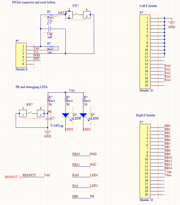
Sheet 1: Microcontroller

Sheet 1-complete
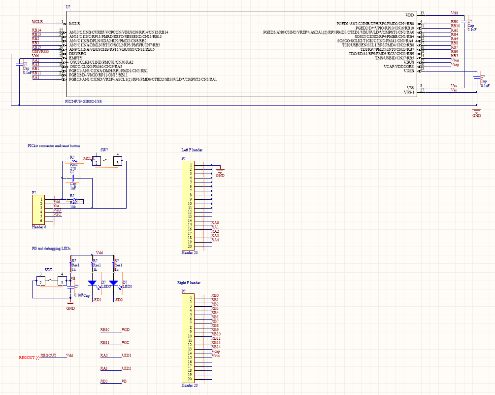
Sheet1-1

Sheet 1-2

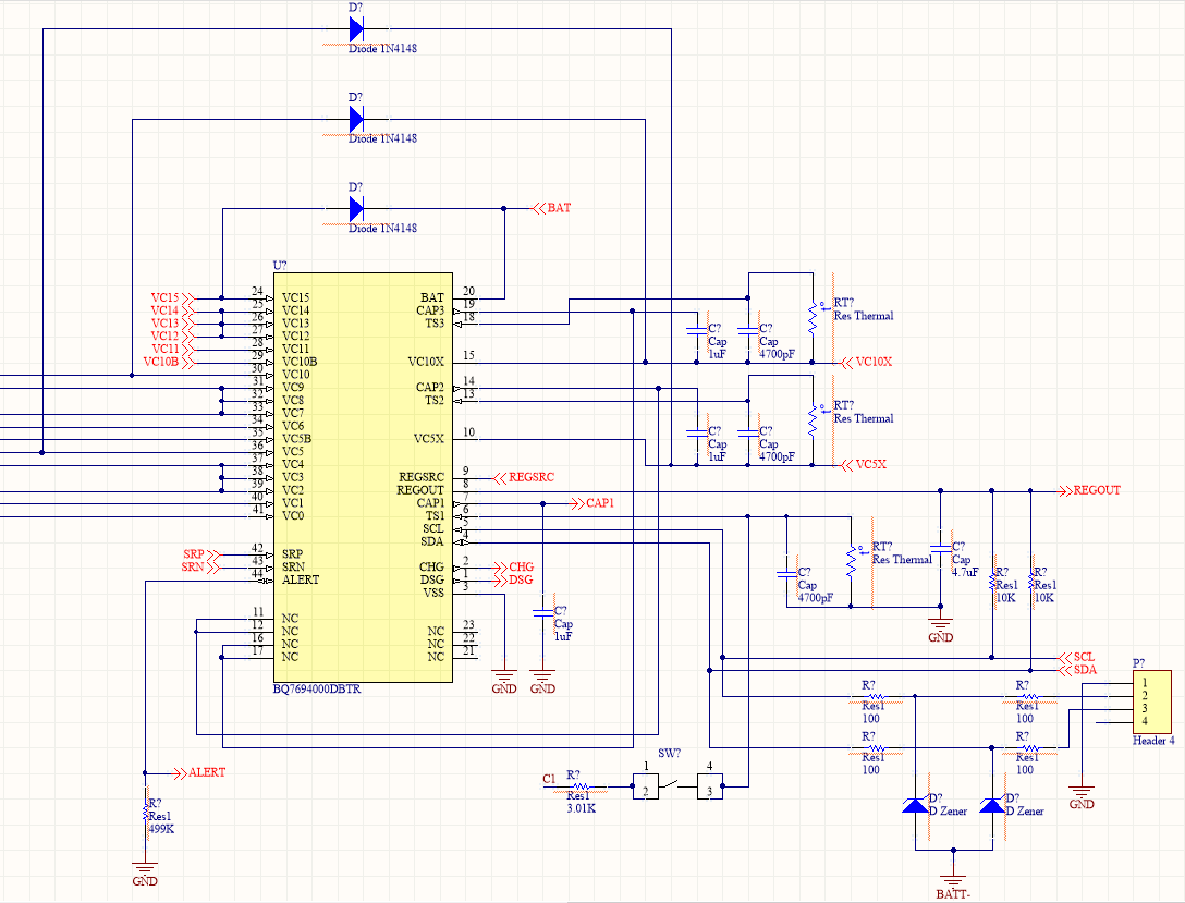
Sheet 2: AFE lower and power out

Sheet 2-complete

Sheet 2-1

Sheet 2-2

Sheet 2-3

Sheet 3: AFE top and power in

Sheet 3-complete

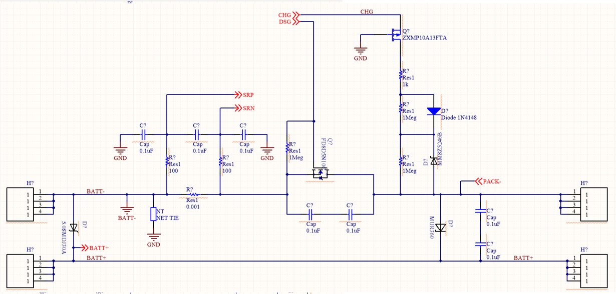
Sheet 4: Power FETs

Sheet 4-complete

Thank you very much,
Robert

  • Hi Robert,
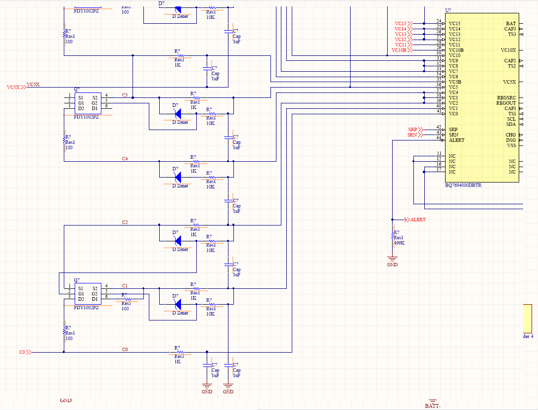
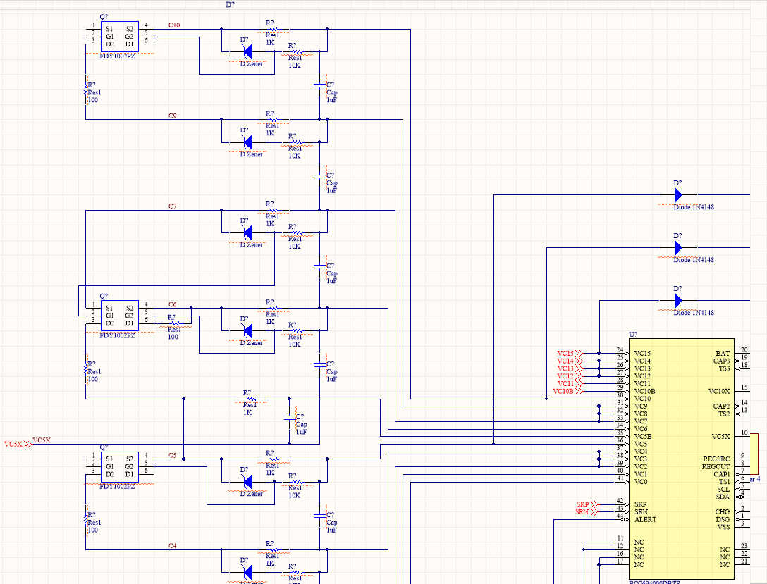
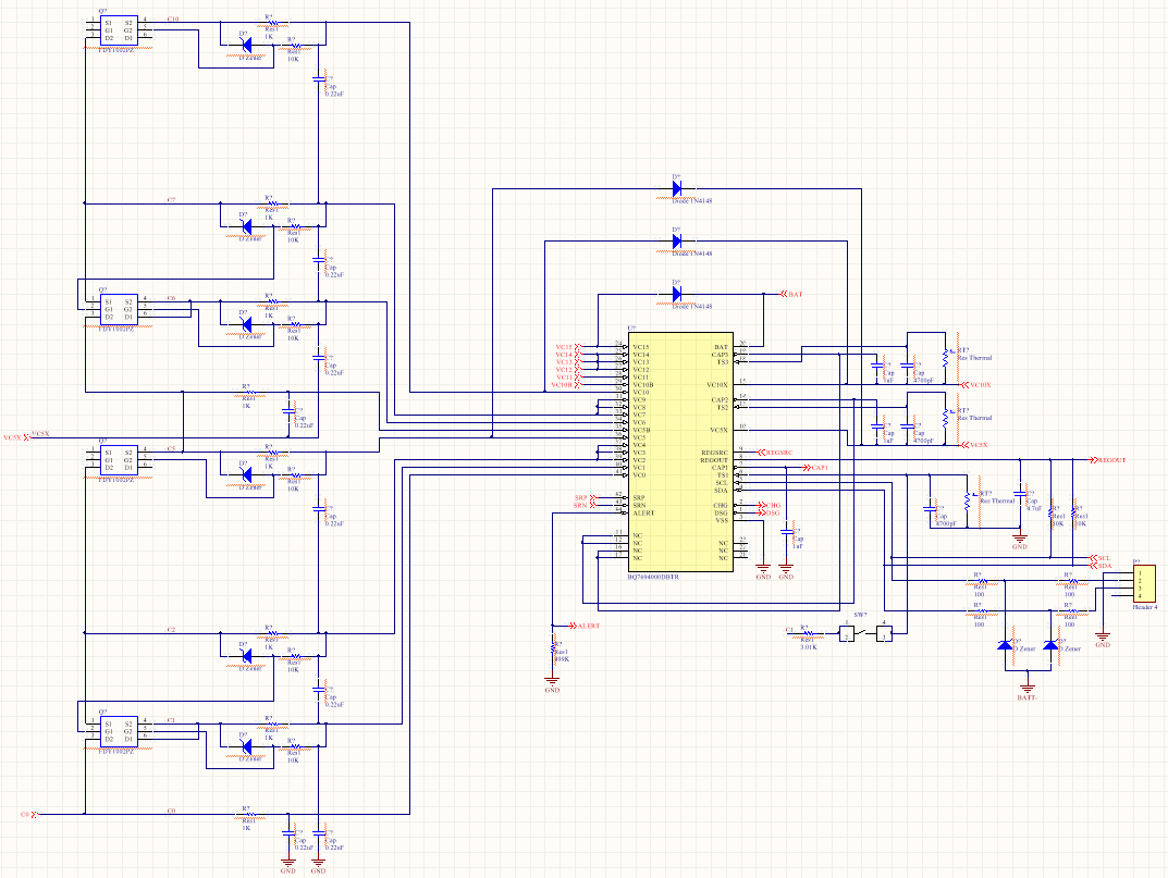
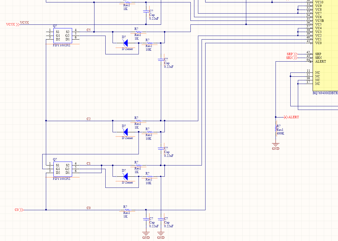
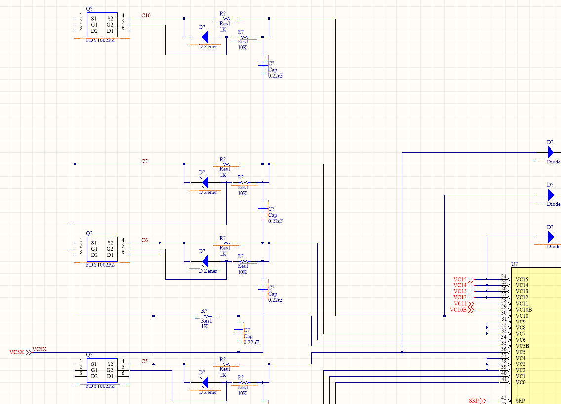
    There are too many input filter/balance FETs for 9 cells. The VCx pins look connected properly for 9 cells, but for example on the bottom group on sheet 2-2 you should have C0 as reference, C1, C2, and C5. Notice that C4 and C2 feed the same net (VC2, VC3, VC4 pins on the IC). Same applies on the middle and upper groups.
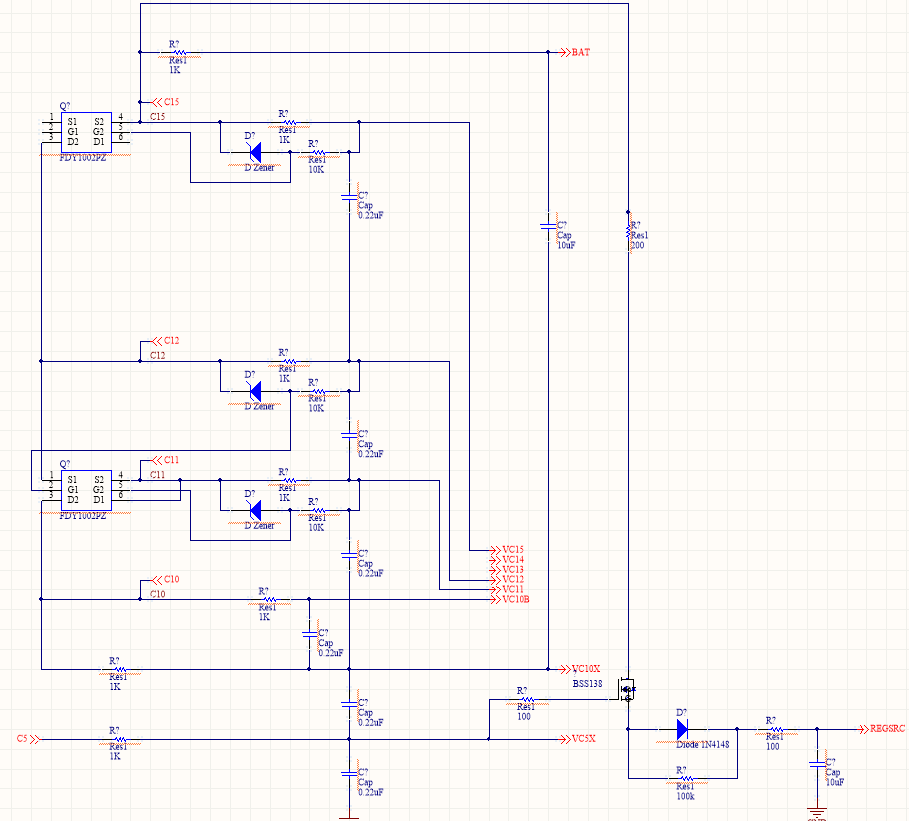
    If you have used the EVM you know that you can see voltage effects from balancing, consider changing the Cc filter capacitors to something smaller than 1 uF. 0.1 and 0.22 have been used in other reference designs.
    The 100 ohm resistors in series with the 1k Rf resistors were current shunt measurement points on the EVM/reference design. You don't need those, the Rf resistor is suitable. When the Rf value was selected as 1k it became a better shunt value without the separate resistor.
    Remember you can support 9 cells with the bq76930, but it will only provide 2 temperature sensors.
    As another reference of this family with a MCU you might see TIDA-00449. Remember that with low side switching isolation is needed for communication coming out of the MCU.
  • Quick question; What are those Es in the schematics (are those jumper ports)? I didn't include them in my schematic.

    >There are too many input filter/balance FETs for 9 cells. The VCx pins look connected properly for 9 cells, but for example on the bottom group on sheet 2-2 you should have C0 as reference, C1, C2, and C5. Notice >that C4 and C2 feed the same net (VC2, VC3, VC4 pins on the IC). Same applies on the middle and upper groups.

    Thanks for pointing that out, I removed those input filter/balance FETs.


    >If you have used the EVM you know that you can see voltage effects from balancing, consider changing the Cc filter capacitors to something smaller than 1 uF. 0.1 and 0.22 have been used in other reference designs.

    I haven't used the EVM before. I've changed the 1uF capacitors to 0.1uF.


    >The 100 ohm resistors in series with the 1k Rf resistors were current shunt measurement points on the EVM/reference design. You don't need those, the Rf resistor is suitable. When the Rf value was selected as 1k it >became a better shunt value without the separate resistor.
    I've removed those as well.

    Did I edit the schematic correctly?

    Sheet 2-complete

    Sheet 2-2

    Sheet 2-3

    Sheet 3

    >Remember that with low side switching isolation is needed for communication coming out of the MCU.

    I'll read on isolation of circuits. Can you tell me how I can implement isolation in this application?

  • Hi Robert,
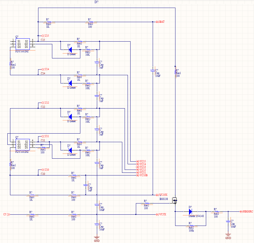
    Your power filter caps on VC5X, VC10X, BAT nets shown on sheet 3 should have stayed 10 uF, otherwise schematic seems appropriate.

    Isolation might be:
    Physical, like the EVM, the control and power go to different physically isolated circuits.
    Switch the communication similar to figure 10 of www.ti.com/.../slua726a.pdf, but don't build a latch. You can't talk to the MCU when protected.
    Use an isolator in the communication path such as U7 in www.ti.com/.../TIDA-01093 although that example is between the (2nd) monitor and MCU rather than the MCU and external system. An isolator requires power on both sides.
    Use high side protection switching such as with www.ti.com/.../TIDA-00792. A high side driver requires power to operate.
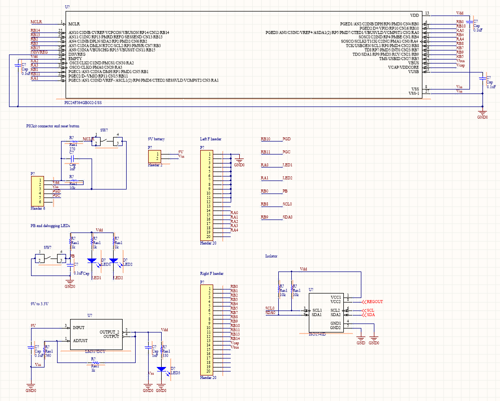
  • Thanks! I've decided to use the ISO1540 for isolation. For side 1 (master), the SCL, SDA, and GND comes from the MCU side (VCC is Vdd which is 3.3V regulated from a 9V external battery source).  For side 2 (slave), the SCL, SDA, and GND comes from the AFE side (VCC is REGOUT from the AFE). Did I build the isolation schematic correctly?

    Sheet1-complete

  • Hi Robert,
    The isolation should typically be outside the MCU/monitor circuit between the MCU and the outside world. This way the communication can float with PACK-, and if the battery is powering the supply for the outside of the isolator that side will lose power when protection occurs and PACK- rises.
    If the isolation is put between the battery MCU and the monitor as I think you have drawn, and the MCU loses power, the battery may not function as desired. For example if the MCU were to start balancing, then a protection event occurs with the MCU off, balancing would continue on the selected cell until the cell was depleted. With the exception of a few protections, the MCU controls the behavior of the battery and needs to stay present.
    It looks like PGC and PGD would be your communication interface to the PIC, but you will know your circuit/system better. If your only output to the outside world is the switch and LEDs, you have the physical & optical isolation and should not need electrical isolation. If something communicates to the circuitry and references PACK-, or if both GND and PACK- come out of the pack, you likely need it.
  • >The isolation should typically be outside the MCU/monitor circuit between the MCU and the outside world. This way the communication can float with PACK-, and if the battery is powering the supply for the outside of the isolator that side will lose power when protection occurs and PACK- rises. 

    Can you please expound on this, I'm sorry I'm really confused about the isolation. If I shouldn't put the isolator between the battery MCU and the monitor as I have drawn, where should I put it? I thought what I did was similar to the sample schematic from http://www.ti.com/lit/df/tidrnc5/tidrnc5.pdf ?

    Thank you for your answers, I appreciate it.

  • Hi Robert,

    Sorry for the confusion.  The isolator in the TIDA is for level shifting, it is the same idea between a comm inside the battery and outside.

    In this picture, the comm path is not isolated, the low side switching causes loss of signal reference and leakage when protection switching is open.  It could also damage components.

    With isolation in the interface lines between the internal MCU and external there is no discharge path when the low side protection is open.  The internal side of the isolator is powered from the pack electronics.

    With high side switching the low side signal reference (PACK-) can be maintained when the protection switches are open.

    Hope this helps.

  • Thanks for the reply. 

    Can you please take a look at my updated schematic:

    Sheet1-complete

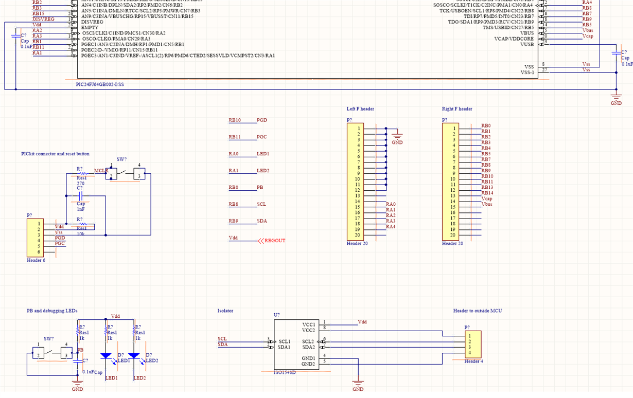
    The MCU is now powered by REGOUT from the AFE. The Isolator side 1 is from the SCL/SDA of the MCU/AFE (I2C pullup resistors are on the AFE side of the schematic), and is also powered by REGOUT from the AFE. The Isolator side 2 is connected to a header with 4 pins, for connection to an MCU outside of the board. Did I get what you were trying to tell me?

  • Hi Robert,
    Yes
  • Thank you very much, I will now proceed to my board layout. I appreciate your help!