A related question is a question created from another question. When the related question is created, it will be automatically linked to the original question.
If you have a related question, please click the "Ask a related question" button in the top right corner. The newly created question will be automatically linked to this question.
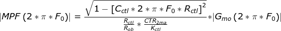
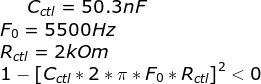
Hi! I am read document slva305c, section 2.9-2.10. Equation to calculate Cctl (38) on page 14. How to calculate the Gmo value that is used in this equation?
Gmo is the Modulator/opto transfer function specified in the 2.10.2. For calculating CCTL in 2.10.3, you would need to set this transfer function equation to 0.75, then work backwards through section 2.10.2 to find the rest of the values used in the CCTL equation.
Are you trying to derive the MPS Plus Filter and Load (MPF) Transfer Function? I recommend going further back in this document to 2.9.1 & working forward from there.
Are you having issues with re-compensating your design? Let me know your requirements & I can recommend proven reference design you can try.
No, I tried to calculate the Cctl value using the value Rctl, Rob and ect. as in the document slva305c.pdf. I did not get the result of 50.3nF. I decided to do the inverse transform to make sure the original values were correct. In the end, I got that the root expression is negative at the specified values.
Yes, I have problems with re-compensating of my design. Schematic is attached. Input voltage: 36-57V, Output: 24V, 540mA When design my schematic, I used applications reference designs PMP8803, PMP5595 and document slva305c.pdf.
Take a look at the feedback values in the attached 23V reference design (PMP21655). Notice R29: it there to make sure the minimum cathode current is satisfied to allow for regulation (see Imin on TL431 datasheet for sizing that R20 resistor). I recommend adding this.
Also, I recommend significantly reducing your output capacitance. Your output capacitor pole may be too strong. For starters, 22uF may be sufficient.
Keep in mind that PMP21655 uses TPS23751, not TPS23753A & is a type 2 design.
C15 is an additional common mode isolation cap like C25. Putting them on the high side of the transformer & the low side (C25) give an additional path for the common mode noise. Additionally, this may provide benefits to EMI performance.