This thread has been locked.

If you have a related question, please click the "Ask a related question" button in the top right corner. The newly created question will be automatically linked to this question.

LM5113: Regarding Delayed Fall time of the part mentioned

Part Number: LM5113
Other Parts Discussed in Thread: LMG1205
Dear Team,
 
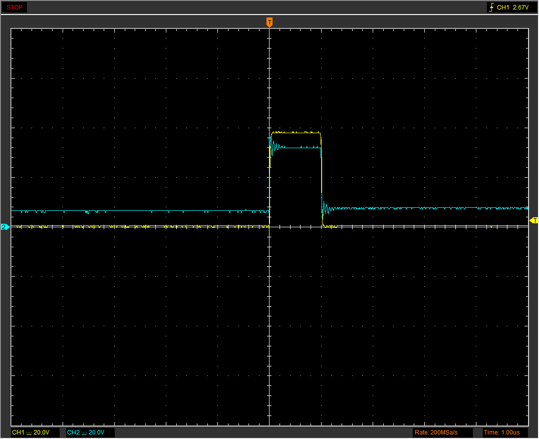
    LM5113 is being used in a FET gate driving application.Following are the circuit componets used & other related details:
 
High Side & Low Side MOSFETs       :  GS66502B-E01-MR
Bootstrap Diode                                : PDS4150-13
Bootstrap capacitor                           : C0402C103J4RACTU(0.01uF,16V)
HOH & LOH resistors                        :  CRCW12065R10FNEA (5.1OHMS, 0.25W) 
HOL & LOL resitors                           :  No Resitor (Short)
 
FET ON Time (nS) Pulse Width (nS) Dead time (nS) Amplitude (V)
HS FET Gate Pulse 1000 100000 10 40
LS FET Gate Pulse 98980 100000
 
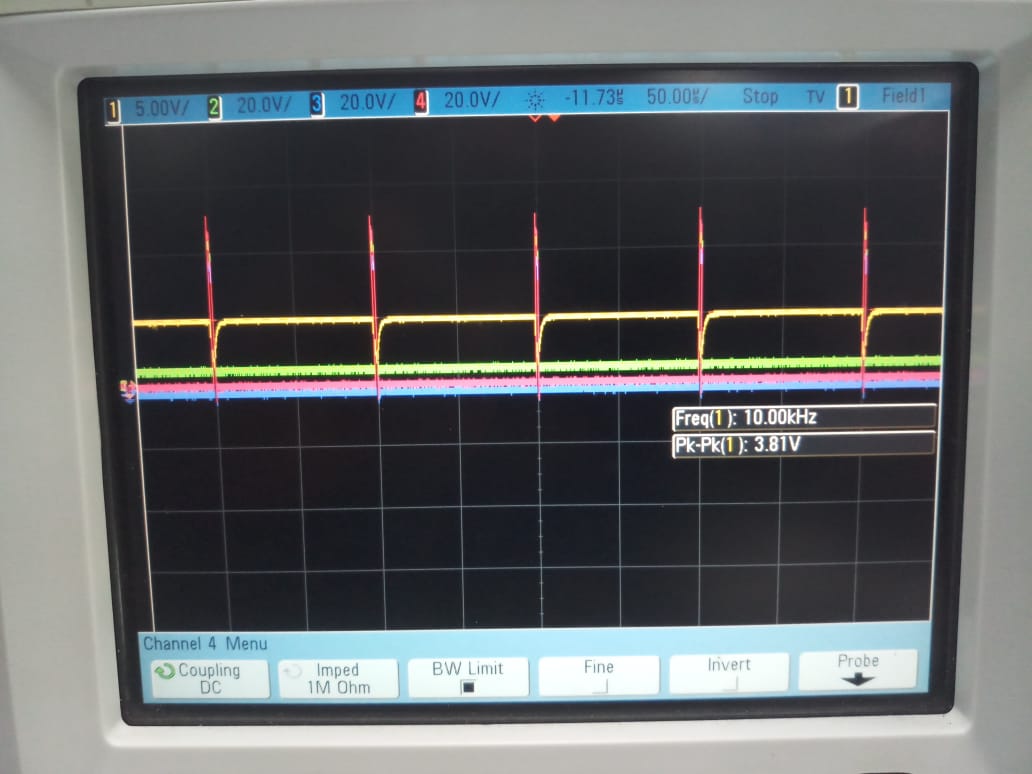
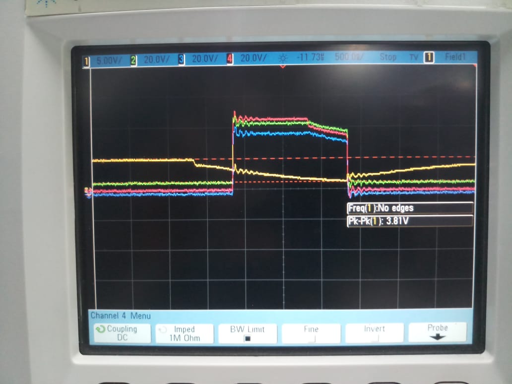
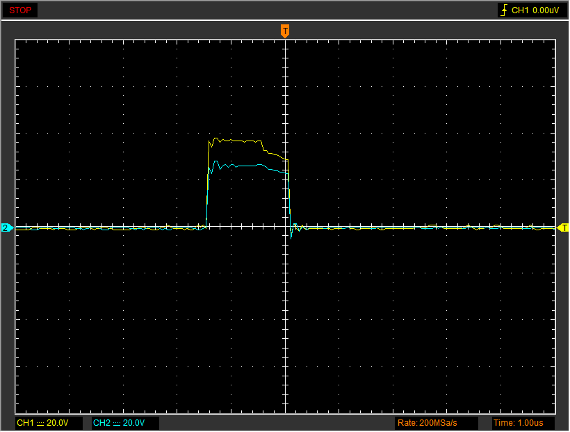
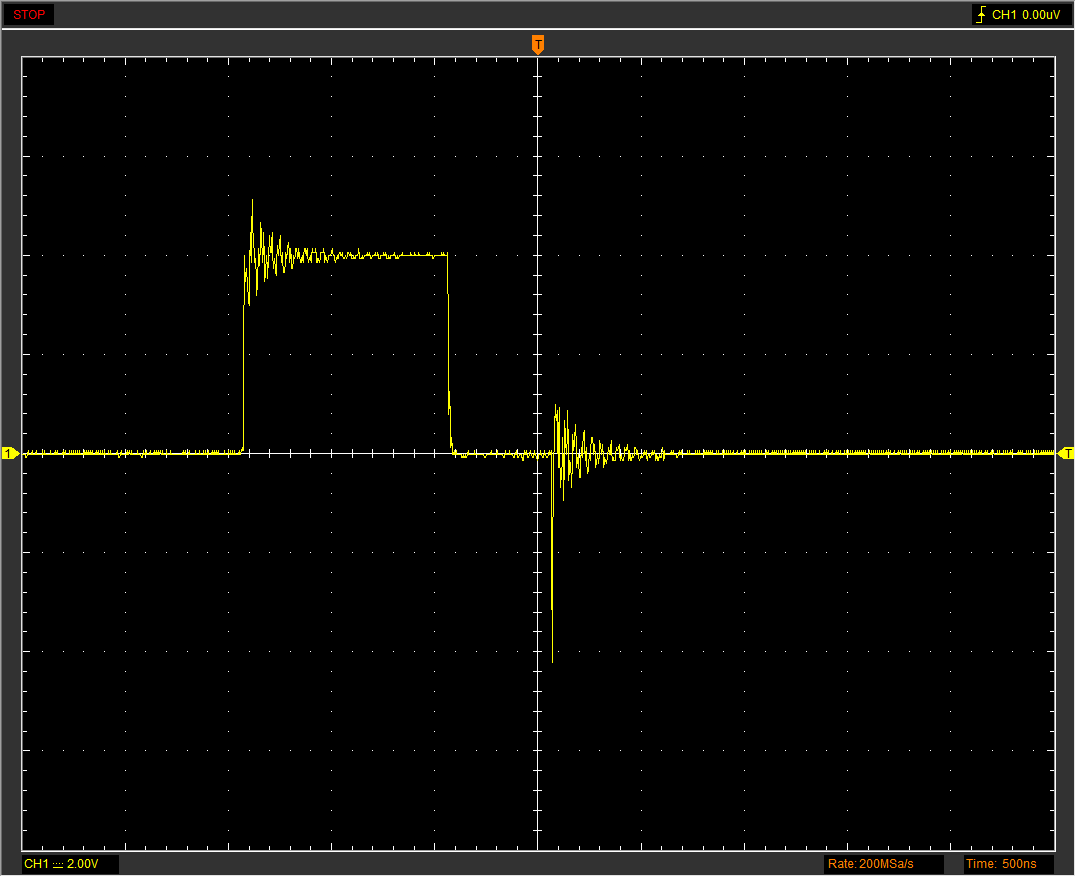
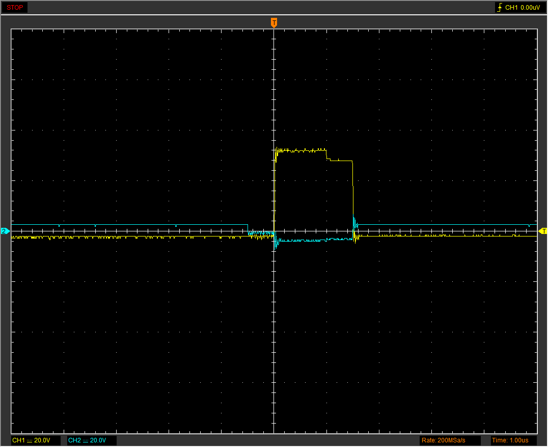
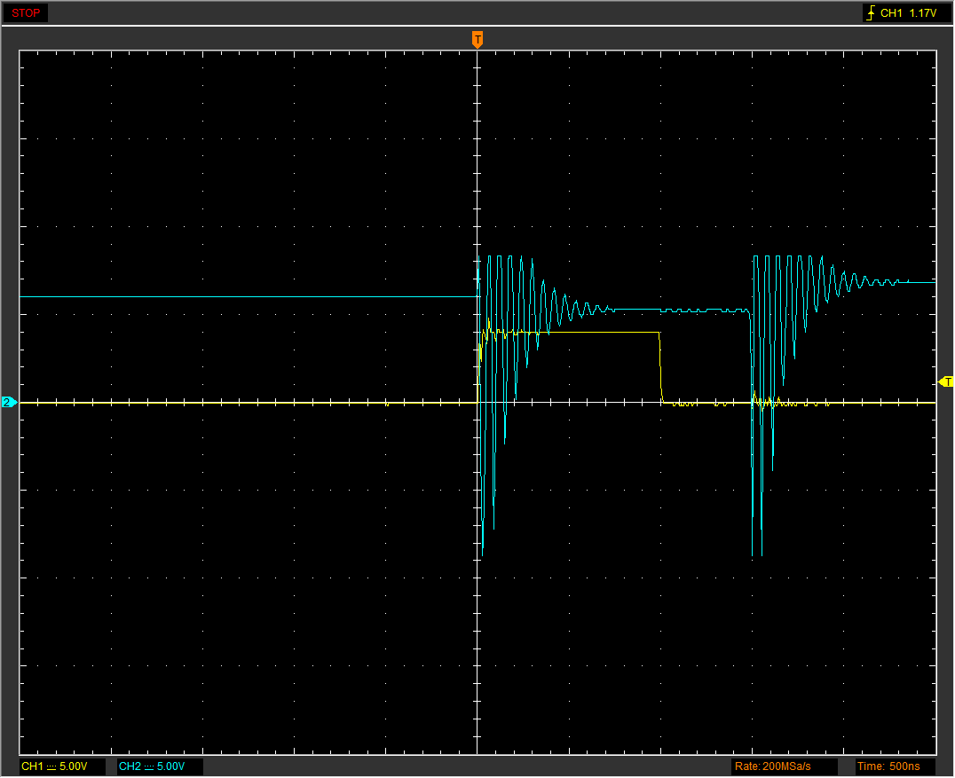
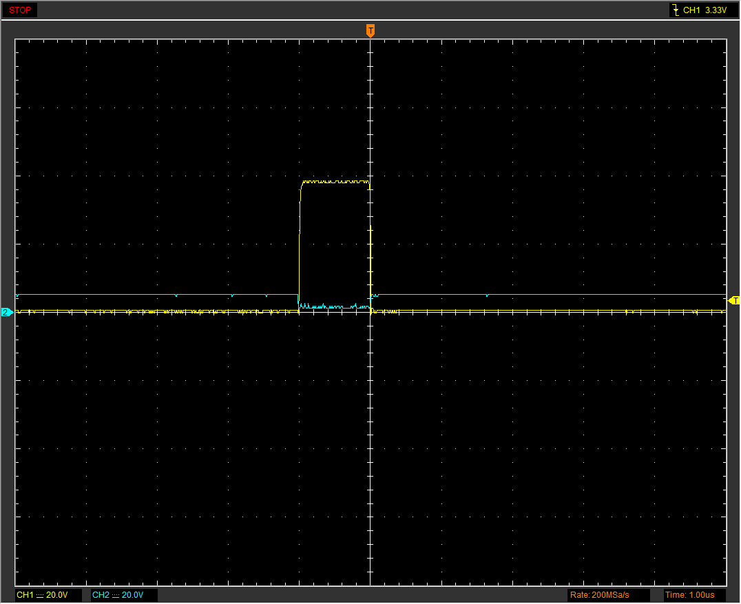
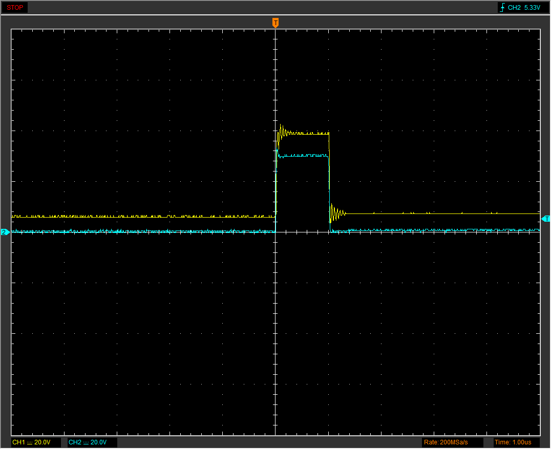
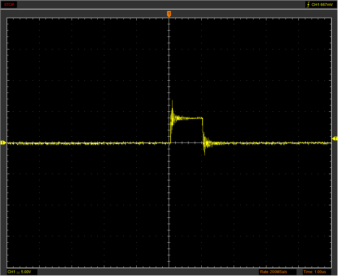
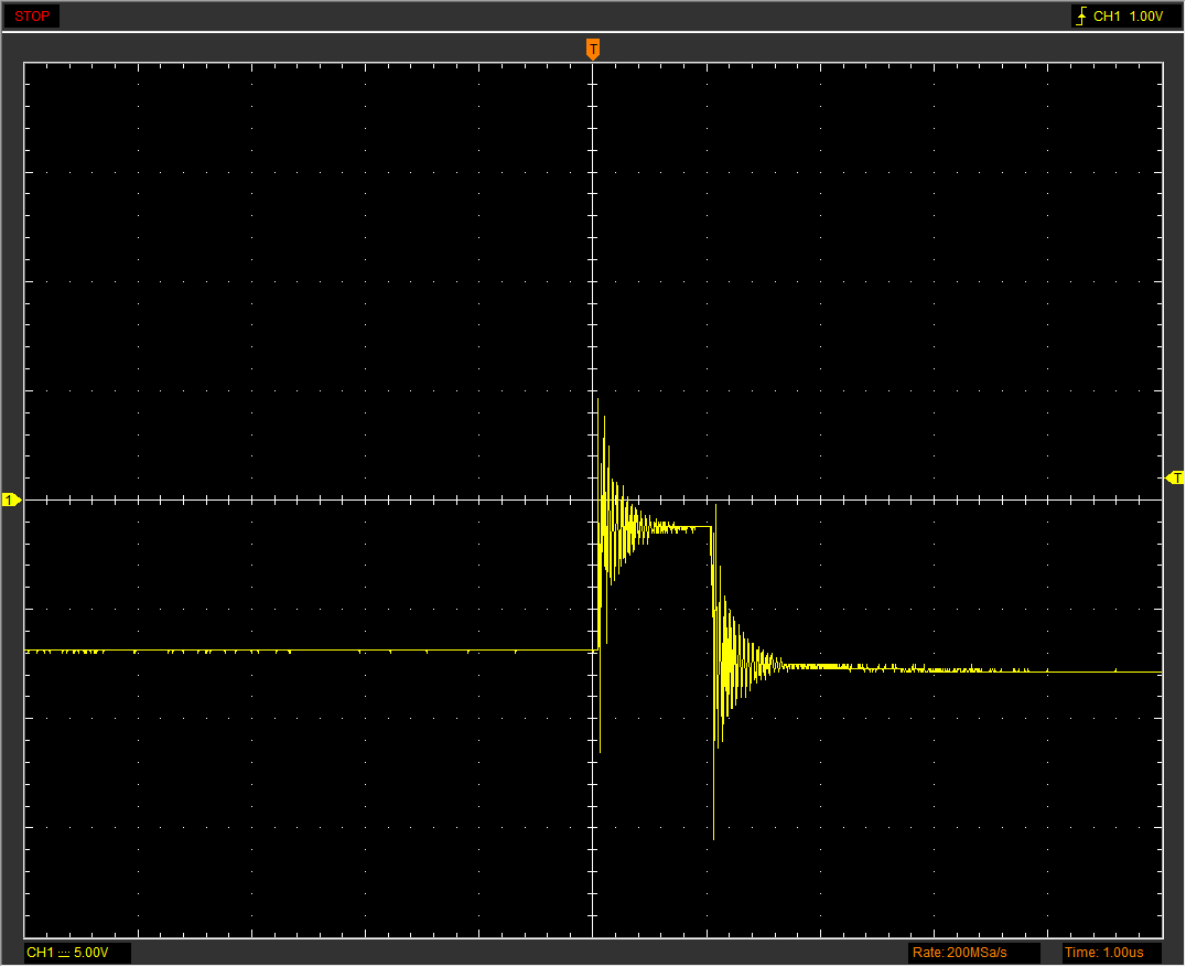
While testing following observation is found:
 
(1)  When output is at No load, High Side MOSFET takes 12uS to Fall from High to Low (Fall time).
 
(2)   When output is loaded to 250mA, same Fall Time becomes 200nS.
 
(3)   While Bootstrap capacitor mentioned above is replaced with CGA4J2X7R2A104K125AA (0.1uF, 100V), no differance is found in fall time.
 
Pl. let us know the reason behind
 
(a) Delayed Fall Time of HS MOSFET.
 
(b) value & voltage rating of bootstrap capacitor to be used.
 
(c) In datasheet a 100 OHMS is recommended to use in series with Bootstrap Diode. but due to our Pulse requiremnt we use a 0 Ohm resiotor. Let us know does it impact the output performance, in any aspect.
 
Regards,
Devarajan R
  • Hi Devarajan,

    Welcome to e2e!! My name is Mamadou Diallo, I am an applications engineer in the High Power Drivers group. I will help address your inquiry.
    LM5113 is not recommended for new designs, have you considered using LMG1205? This device has the same pinout and better performance for your design. I would first recommend using LMG1205.

    Second, can you share a snippet of the gate drive portion of your schematics along with the captured scopeshots? The reason I am asking for the schematic is to review your bypass capacitor values along your bias supply which also important parameters for good bootstrap bias performance. What is your VDD? I assume you're using 5V, can you confirm? I assume you have a Vbus voltage of 100V can you you confirm as well?

    -The delayed fall time of the HS FET is likely due to the choice of bootstrap capacitor's value used. Your bootcap value seems too low based on your FETs. This cap should be sized to be at least 10X your calculated bootcap: Cboot (abs min) = Qg / ( VDD - Vhbr - Vhbh) where Qg = 1.5nC = gate charge ; Vhbr - Vhbh = HB rising threshold (max) - HB threshold hysteresis = 3.9V - 0.2V and VDD I assume = 5V. Your bypass cap accordingly should be sized such that Cvdd = 10X Cboot.

    Section 8.2.1 of the LMG1205 datasheet gives an example calculation for the bootstrap circuitry.
    www.ti.com/.../lmg1205.pdf

    The bootstrap resistor influence the charging of the high side fet such as the charge time for the bootstrap supply essentially follows the exponential behavior of a typical RC circuit where Vhs,FET = VDD * (1 - e ^ (-t / Rboot * Cboot)) therefore 0-Ohm would increase the peak current to charge the high-side FET turn-on time.

    Please take a look at LMG1205, which is our recommended replacement for this device.

    Thanks.

    Regards,

    -Mamadou

  • Hi Devarajan,

    Thanks for the scopeshot.

    Are you restricted to using this device? I would highly recommend switching to LMG1205 as you may not be getting the best driver for your design.

    On your schematics, is the HB left floating or connected to the bootstrap capacitor and diode? Can you confirm?

    It looks like shoot-through may be occurring from the excessive ringing on the low-side FET gate during the rising edge of the high-side FET. It looks like it is also occurring on the slow falling edge of the high-side FET.

    Is the high-side FET signal referenced to HS pin? Are you using a differential probe to capture HO-HS?

    Can you capture 2 or 3 periods of the following signals: HB-HS (boot cap supply) also using a differential probe? as well as LO (low-side gate) and HO-HS ( high-side gate also using a differential probe) on the same scale.
    Then a zoom-in on full period similar to the previous scope shot.

    Again i would suggest using a different driver as this issue could be the result from using this driver given that this device has been NRND(not recommended for new designs) rather than being the root cause of the problem.

    Thanks.

    Regards,

    -Mamadou
  • Hi Devarajan,

    thanks for your question on LM5113, Im an apps engineer who works with Mamadou, let me try to help answer your issue.

    In the schematic the anode of the bootstrap diode and the + of the bootcap should be connected to HB, can you confirm this?
    for an example schematic check out the LM5113 front page of the datasheet.

    Is your load inductive or resistive? It looks resistive as the 200ns fall time is an RC time constant with the output capacitance and your load size. This is normal with a 250mA load since during turn off the switch node can only discharge back to 0V in the amount of time it takes the load current to charge up the highside Coss and traverse through the resistive load. does the fall time get even better with higher load current? whats your target fall time? what does this mean for you application's perspective (is this for motor drive)?

    It also looks like you have some parasitic inductance and maybe capactiance in your board layout. Can you show me your layout for review?
    Thanks,
  • Hello Team,

    In the schematics, cathode of the Bootstrap Diode &  +Ve of the Bootstrap capacitor are connected to HB pin.

    Pl. find the scopeshots attached as per your request.

    Note:All shots attached are captured with respect to GND.  HS FET's Gate signal & Bootstrap capacitor +ve terminal with referenced to HS shots will be attached shortly;

    Colour of signals in scope shots:

    RED Colour:  HS FET's GATE

    Green Colour:  Bootstrap capacitor's +ve terminal.

    Blue colour:  HS Pin / HS FET's Source

    Yellow: HS FET's GATE

  • In continuation to previous attachment:

  • Hi DEVARAJAN,

    thanks for your update,

    what is the red and yellow trace? are they both 'HS FET gate' in your description.

    I notice that your bootcap is smaller than usual and there might be an issue with the charging or discharging seen in your next scope shots, LM5113 datasheet section 8.2.2.2 helps with bootstrap cap calculation

    does the issue get better if  you try a 0.1uF bootcap?

    Thanks,

  • Dear Team,

    Thanks for your reply.

    Red colour is HS FET's Gate signal and Yellow colour is LS FET's Gate Signal.

    Initially  C0402C103J4RACTU/CAP CER 0.01uF 16V 5% 0402 X7R +/-15ppm was used as Bootstrap cap. Then it is replaced with CGA4J2X7R2A104K125AA  / CAP CER 0.1uF 100V +/-10% X7R 0805 RoHs AECQ200. But no difference observed. Wave form attached for your reference is taken with latter (0.1uF/100V).

    Pl. find the HS gate & Bootstrap capacitor supply with referenced to HS pin scope shots.

    While measuring HS Gate-HS pin i found no delay in the fall time & just the ringing;  I can understand it as "once HI pin becomes low HS gate is pulled down toHS pin through HOL pin". But at the same time i measured both HS pin & HS gate with referenced to GND. there again i found the delay in fall time. What it mean actually? Because if  what i mentioned in quotes is the case, then while measuring with respect to GND also there should not be any potential difference between HS gate & HS pin once HI becomes low. Right?

    Note: Blue  : BOOTSTRAP capacitor wrt HS pin;   Yellow is HS gate wrt HS pin

     .

  • Scope shot : Yellow colour : HS gate wrt HS pin & Blue colour  : Bootstrap capacitor supply wrt HS pin.

  • Scope shot : Yellow colour : HS gate wrt HS pin & Blue colour  : Bootstrap capacitor supply wrt HS pin.

    In this waveform, as we can observe  there is no delay in Fall time. Wave form is restricted to 1uS what i configure.


  • scope shot 3: Blue colour: HS pin  wrt GND & Yellow colour : HS gate with respect to GND.

    Here we can observe the delay of 0.5uS which is nothing but the deadtime set between HI & LI pulse.

  • Hi Devarajan,

    since the yellow is the LS output,
    for the waveform [pk-pk(1):3.81V] I notice that LO output is really slow rise/fall time.
    can you confirm the resistance on the board on LOH/LOL to be 5ohms and 0ohms respectively?

    does this long rise/fall on LO get faster when you change the duty cycle to be shorter?
    can you show the load current to see if there is shoothrough that might have damaged something or thats lifting the source of the HS FET to the point where you see the drive voltage slowly decay?

    thanks,
  • from the waveform of HB ringing in ble and yellow,
    are you probing with a pigtail method to reduce loop inductance into the measurement?
    if this is the true ringing peak value then its possible the driver is damaged.

    can you send you layout for a review to make sure the HB cap is closed within close proximity to the HB-HS pins?
    its possible that the bootcap is being over charged due to the layout ringing keeping the internal bootstrap switch on.
    in order to tell if the bootstrap is being overcharged, pigtail probe HB wrt HS ; can you also probe LO and HO on the same plot where everything lies in the switching cycle (zoom in to only 1 or 2 cycles with same V/div scaling)?

    thanks,
  • Hi Devarajan, 

    Looking through your screencaptures, I suspect that the most likely explanation of the scope shots you are seeing is that the part is correctly pulling the high-side gate output down quickly when commanded as you see in the measurement when you use a diff-probe to measure HS-Gate to HS. I suspect that in the scope capture where you plot the HS-Gate and HS signal on separate scope channels is incorrect. In particular, I suspect the two probes were not quite perfectly compensated when you did that measurement which could show the data you are seeing. If you look, the HS-Gate signal does drop by about ~4V when it is supposed to, it just does not drop to HS, but I suspect that is because of poorly compensated probes.  The HS voltage itself drops slowly because you have little load on it to pull it down. If there is no load, HS will just stay high until the low-side turns on and pulls it down which is what you are seeing.

    One thing that did catch my eye is in the plot where you plot the LS-Gate on the yellow, it does not seem to fall rapidly when the low-side shuts off, instead it seems to have alot of resistance in the gate-drive path. If this is real, it will cause shoot-through when the high-side turns on and could be responsible for the high ringing seen when the high-side turns on. I would double check this and see if the low-side gate is being driven up and down quickly. However, in your first attachment, a scope capture shows the low-side gate being driven quickly, so this seems to contradict this.

    Regards,

    Nathan

  • Dear Jeffrey & Nathan,

    I thank you for reply & effort taken to solve the issues.Request you to wait for few more days for my reply as the board is used for another testing.

    Regards,

    Devarajan

  • Hi Devarajan,

    thanks for your update, I will mark this thread as resolved for now... but you can reopen the thread by replying when you want to relay your test results any time you want.

    thanks,
  • Dear Team,

    Thanks for continued technical support.

    As Mr. Nathan pointed out, there is no delay in Fall time of the HS Gate. It is clearly a measurement error.

      And as Mr. Jeffrey instructed i followed Pig tail method (Using Ripple TIp) while probing  both HS Gate & BS cap supply wrt HS pin. But no improvement is observed  in Ringing. So Iam planning to provide a capacitor across Bootstrap Diode to reduce ringing. Kindly suggest is that recommended?

    For your kind reference, this time i tried to eliminate all measurement errors & attached captured waveforms.

    Also my pulse requirement is 10nS ON time, 50nS Pulse period, 10nS Deadtime. Pl. suggest will it work with the schematics i sent you. Why because I continuously face  MOSFET heating & followed by long term failure when it is operated at configuration mentioned.    I suspect heating is due to direct short of supply to GND through both FETs. Even sometimes i  used to hear a sound from MOSFET & suspect that is due to over current flowing through FETs during short event. Is it this ringing we are specking about is responsible for that too??

    And for kind notice i have requested my seniors for sharing Layout file and waiting for thier reply.

    Regards,

    DEVARAJAN R

  • Wave form 1 : HS FET gate wrt HS pin

    No Delay in fall time; Configured ON time is exactly 1uS.Configured dead time is 500nS

     wrt 

  • Scope shot 2 : Yelow : HS gate & Blue : LS gate

    No Delay is observed in LS gate Turn OFF & Turn ON. Previous one may be due to Measurement error as MR. Nathan pointed out.

  • Scope Shot 3 :  Yellow : HS GAte; Blue is BS cap supply wrt HS pin.

    What causes Ringing???

    Second ringing may be due to LS Gate turning ON

  • Hi Devarajan,

    The HS gate waveform looks good without too much ringing. The LS gate waveform looks suspicious. It only goes to 3V when it is on? it goes to -4V when the high-side is on? This is suspicious. You may try probing the low-side VDD to see if it is also moving, if so I'd suspect something with your grounding/probe/setup maybe a problem.

    On the graph where you show the HB-HS waveform in blue, I'm also suspicious that something is wrong. It is showing the HB-HS supply goes to 6 & 7V, but I don't think that is real because the differential high-side gate measurement only goes to 4V. This means that when the high-side is on, the HB-HS voltage should be the same, or 4V. Since your blue curve shows it is over 5V at this time, I'm suspicious of the measurement. How are you doing the measurement? Do you have two diff probes to measure HB-HS and HGate-HS at the same time? If so, can you flip the probes and get the same result? Maybe they are different model probes and one has much better CMTI rejection than the other which could cause what you are seeing.

    Do not put a cap across the bootstrap diode, that will make HB-HS ringing worse and add lots of losses to the power FETs. The bootstrap diode should be a very low capacitance type with no additional capacitance.

    Nathan
  • Scope shot 1: Yellow is HS Gate HS pin &  Blue is LS gate wrt HS pin

  • Dear Nathan,

    As instructed, i found no variation while interchanging probes for  HS Gate & BS cap supply wrt HS pin measuremnt. Waveform is exactly same as what i shared yesterday.

    But same measuremnt i took wrt GND. I mean  HS Gate wrt GND & BS cap supply wrt GND. In this measurement while interchanging probes i could observe the variation. But ringing seems to remain same.

    Regards,

    Devarajan R

    Scopeshot 2: Yellow is BS cap wrt GND & Blue is HS gate wrt GND. In this waveform BS cap supply is higher.


  • Scope shot 3 : Yellow is HS Gate wrt GND & Blue is BS cap supply wrt GND. In this waveform, Bootstarp is lower than HS gate.

    Why not this variation is observed while probing wrt to HS pin. 

  • Dear Team,
    For your information configuration details below:
    ON time of HS pulse is 1uS; Pulse period of HS pulse is 100uS.
    Deatime b/w HS & LS pulses is 10nS.

    And i just request you to clarify whether ringing is the cause for Heating/ failure of HS MOSFET.

    regards,
    Devarajan R
  • Hello Nathan,

    To just confirm that voltage rise(over charging) of BS cap supply to 6V/ 7V is not due to measurement error i probed each signal separately with single probe and the same result.

    Scope shot 1 : BS cap supply wrt to HS pin

  • Scopeshot2 : HS gate wrt Hs pin

  • Scope Shot 3 : HS Gate wrt BS cap supply.

    From the last 3 scope shots, i could infer the following: (1) Before HS FET turns On , BS cap supply is at 6V (2) When LS FET turns ON, BS supply is at 7V. (3) When HS FET turns ON BS Supply is 1V below HS gate. (4) As Mr. Jeffrey pointed out, BS cap may overcharge due to parasitic inductance in the trace.

    Pl. clarify (1) why 1V difference arises between HS gate & BS cap supply pin when HS FET turns ON?or is that normal? (2) Is there any solution to solve this overcharging without changing routing? (3) is this overcharging & ringing in BS cap causes heating/ failure of High FET.I mean does this turn ON both MOSFETs at same time?    

  • Hi Devarajan,

    I can't think of any reason why the the high-side gate and the bootstrap supply pin would be different when the high-side is on. Do you have a pull-up gate resistor? If so, can you probe across it (or do two measurements, one on either side of it) to see if there is a voltage drop across the resistor?

    Regarding the ringing on HB and the higher than expected voltage on it, I'm suspecting it is your bootstrap diode. You show you have a zero ohms in series with your external bootstrap diode, and the bootstrap diode is very large with a large capacitance relative to the rest of your system. For example, the bootstrap diode PDS4150-13 at 5V reverse bias has 200 pF of capacitance and more at lower voltages. Compare that to your FETs which only have between 18 and 125 pF depending on voltage, and it is clear you are maybe doubling your Coss switching losses by adding that diode. This could be why the FETs are getting hot (the additional loss caused by the diode will appear as switching losses in the FETs even though the capacitance of the diode is the problem). This capacitance would also greatly increase ringing on HB which you are observing.

    For the diode, I'd recommend a very small diode with a larger series resistor. In general, you can rely on the internal diode of the LM5113 for the bootstrap, the external diode is only present to help at start-up (the LMG1205 does not need this help at start-up so it does not need an external diode). Because it only serves a limited purpose, put a very small diode maybe a BAT46 or similar which has less than 10 pF of Coss at low voltages. I'd recommend a 10-100 Ohm resistor.

    Regards,

    Nathan

  • Dear Mr.Nathan,

    Thanks for your reply. Overcharging issue of bootstrap capacitor  is solved by implementing your suggestion. Previous Diode (PDS4150-13) is replaced with BAT54SLT1G. Now i think ringing & overcharging of BS cap is solved. Wave form is attached fyr.

    But still heating of High Side MOSFET din't get solved. As the ON time & total period of pulse is reduced, heat of Hs FET increases. What might be the cause?

  • In continuation to last upload:

    Also i hear a ringing sound from HS GaN FET in addition to heating. What would be the cause?

    Scopeshot 1: BS cap wrt GND. Hope BS cap supply is clear.

  • Hi Devarajan,

    In general, the power dissipation of the high-side MOSFET is caused by one of the following:

    1.) Conduction losses (I^2*R*D) losses where I is the current, R is the rdson of the FET, and D is the duty cycle

    2.) MOSFET Qoss losses = Qoss*V*Fsw Where Qoss is the Qoss of the FETS+PCB, V is the bus voltage, and Fsw is your switching frequency.

    3.) Cross conduction losses during switching: proportional to load current, bus voltage, switching frequency and inversely proportional to transition time.

    4.) Possibly shoot-through losses. Should not normally occur, but could occur if both FETs are turning on at the same time.

    Though you haven't told me your current, but i suspect it is low from previous discussions, so I don't expect issues from 1 or 3. The gate waveforms look like they are non-overlapping so 4 should be eliminated unless there is lots of inductance between the driver and the FETs which could cause the FETs to turn on even when the driver is trying to hold them off.

    For (2), your switching frequency is low enough  (100 kHz correct?) that the Qoss of the FETs will not be large enough cause lots of heating, but what is the load connected? Does it have lots of capacitance. Typically a half-bridge has an inductor connected which has some capacitance but not too much, however you have never spoken about the load. Is it something other than an inductor? What is its capacitance?

    The audible noise is probably from ripple on a ceramic capacitor. Ceramic capacitors are somewhat piezoelectric which means they deform in response to an electric field. This means that ripple voltage on the capacitor in the audible frequency range can make the capacitor flex at that frequency and can be heard. However 100 kHz is above audible range. Maybe there is another lower frequency ripple in the system somewhere?

    Nathan

  • Hello Mr.Nathan,

    Thanks for your forum support.  I calculated Losses in HS FET & observed that it is the Qoss Loss that dominates for the following configuration:

    Qoss = 14.2nC (from datasheet)

    Bus Voltage = 40V

    Pulse period =200nS (Frequency = 5MHz).

    I could understand  by reducing Voltage / Frequency, this loss can be reduced. Is there any other solution other than touching those parameters.

    Output is at No-loaded condition & above is the operating configuration in which i observed heating of HS FET.

    Regards,

    Devarajan R

  • Hi Devarajan,

      I didn't realize you were trying to switch at 5 MHz. 5 MHz hard switching with a 40V bus will result in high losses and there is not much you can do about it. You can switch faster with a soft-switching topology but that requires a major change to a new topology. Regretfully, there is no way avoid dissipating the Qoss loss when hard switching.

    Regards,

    Nathan

  • Hello Mr.Nathan
    Thanks for your reply.
    Finally one doubt I have. While switching with bus voltage of 40V, almost 5v drops across HS FET and only 35V appears in output. I suspect the drop is due to QOSS loss. Am I right?
    Regards
    Devarajan R
  • Hi Devarajan,

     There should only be IL*Rdson across the high-side when it is on. If there is more than that, something is wrong. It could be a measurement issue (probe compensation again) or maybe some unknown load. Is the supply current normal?

    Regards,

    Nathan

  • Hi Devarajan,

    It's been a while since we've heard from you, so we must assume you've resolved your issue.

    If possible, please post how it was resolved for others to learn from.

    If your issue isn't resolved, let us know, and we will work with you to resolve it.
  • Hi All,

    This discussion helped me to clearly understand the working of LM5113 IC. I thank you all for the support. Especially i thank  Mr. Nathan as he pointed out  the  probing errors i made,provided a  solution for over-charging of bootstrap capacitor & pointed out Qoss Loss in HS FET. Hopefully his reply took debugging in right path & solved all issues.Thank you all.

    I din't solve  high Qoss loss instead just reduced it by operating at lower voltage. All other issues & solutions are available in forum.

    Regards,

    Devarajan R