This thread has been locked.

If you have a related question, please click the "Ask a related question" button in the top right corner. The newly created question will be automatically linked to this question.

TPS63020: Unexpected dynamic current limit in step load response

Part Number: TPS63020

Dear All,

I'm writing to enquire about a problem with the TPS63020 DC-DC converter.

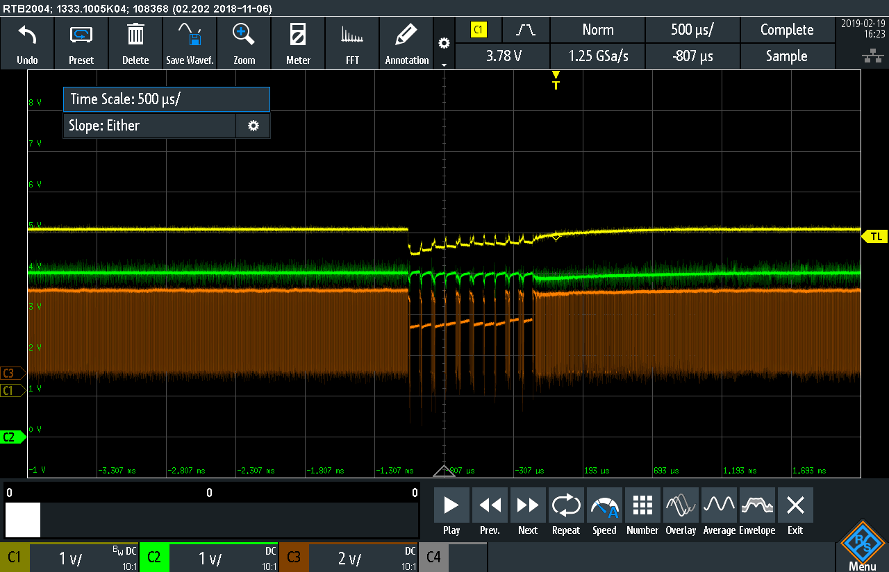
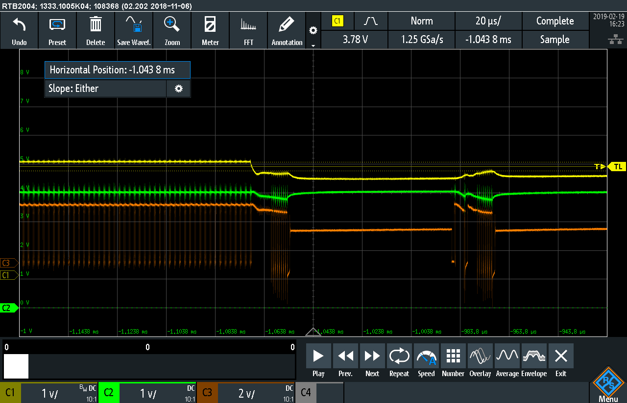
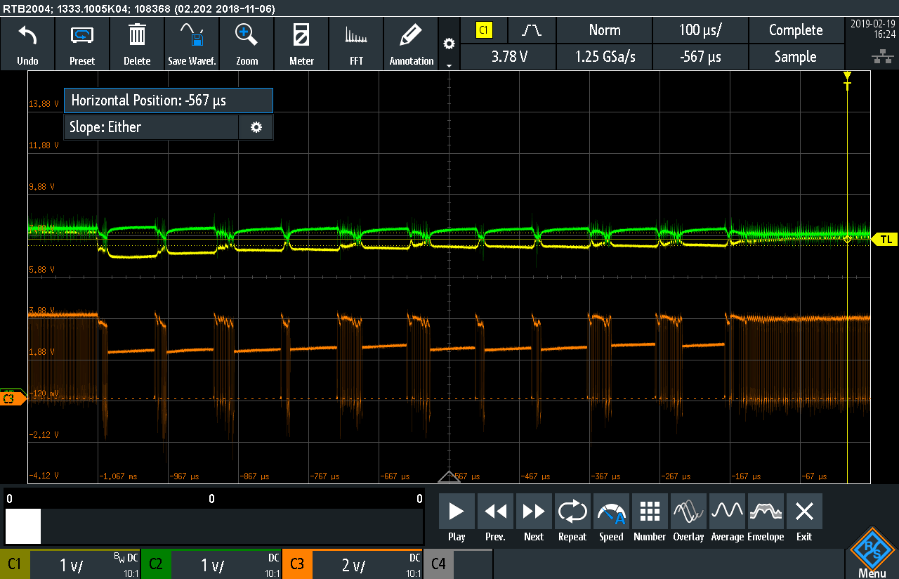
I tested the component on our board with a step load test, with a constant resistive load (25ohm) and an additional low resistance load (5ohm) connected with a n-channel mosfet, that is open for a short amount of time.

When we connect the 5ohm resistance, the DC-DC converter enter in burst mode similar to the one described in chapter 7.3.2 of the datasheet and the output voltage becomes to low for a correct operation of the whole device.

Please find attached the screenshots of the oscilloscope.

Regards,

Andrea Bedin

Yellow trace: Vout;
Green trace: Vin;
Orange trace: Voltage on pin L2.

  • Hi Andrea,

    Could you please post the schematic, or at least specify the operating conditions (Vin, Vout, Iout)? How much does your system differs from the EVM and did you follow all the recommendations for the PCB layout and minimum input/output capacitance? Also, what are you using as the input power supply?

    Looking at your scope plots, it seems that you have Vin=4 V, Vout=4 V, Iout=160 mA + 800 mA pulse? Testing the TPS63020 under those conditions on the EVM does not show any problems, just one short -150 mV output voltage transient.

    Best regards,
    Milos
  • Hi Milos,

    we can't post the schematic here because is part of a confidential schematic (i can share it only by private message). I can list the operating condition of the device.
    The output is setted to 4.2V and the input is variable (from 3.5 to 4.3V,  in the final design we will use a Li-Ion battery). During the test we are powering the board with a linear DC power supply with voltage 3.7V (max current 4A).
    The input capacitance is about 240uF (220uF+10u+10u+56p). Both the 10uF capacitors are close to the output of the converter. The output capacitance is made by 47uF+220uFx2+5x56pF, approximately 500uF.

    PS pin is asserted, and the feedback track has length a couple of millimeters.

    The load pulse we tried is from a current of 170mA to 840mA (5ohm resistor).

    When we apply the load resistor, the output voltage drops 300mV and the regulator doesn't compensate this error since the pulse is ended. If we add a 100uF electrolitic capacitor in parallel to the 5ohm resistor (to simulate a resistive-capacitive load), the response is even worst.

    I've just checked the load pulse response shown in Figure 5 of SLVU365, but our is different. (Green: Vout, Blue: Vin, Yellow: PIN L2, Orange: Load activation command).

    We tried to add some extra capacitance before and after the DC DC converter, and this doesn't help to solve the problem.

    Andrea Bedin

  • Hi Andrea,

    Could you please post the schematic and the PCB layout to lbs_request@list.ti.com.

    In the meantime, I will try to reproduce the same behavior on the EVM.

    Best regards,
    Milos

  • Hi Milos,

    we have sent to You an email with the schematic and the PCB.

    Kind Regards,

    Andrea

  • Hi Andrea,

    Thank you for the schematics and layouts.

    As noted before, there were no issues testing the same load pulses on the EVM. In your case, a possible reason might be the impedance before the TPS63020. Unless you have tens of mF of capacitance, 800 mA current will quickly deplete the charge of your input/output capacitance and then your source might limit the current or cause the voltage drop. Could you please try powering the TPS63020 directly with a bench supply, to make sure nothing on the PCB is limiting the input current?

    Looking at the PCB, the ground routing around the TPS63020 should be significantly improved. As it is now, there is a large and long loop going from PGND pins below L1 and then to GND fill. Please add multiple GND vias as close as possible close to the PGND of the TPS63020 and GND ends of the input/output capacitors (C92, C93, C94). Small input/output loops are crucial for the stability of switch-mode converters, especially during transients. Please take a look at the recommended layout in the Figure 29 of the datasheet, and try to stay as close to it as possible.

    Best regards,
    Milos

  • Hello Andrea,

    I haven’t heard back so I’m assuming you were able to resolve your issue. If not, just post a reply below (or create a new thread if the thread has locked due to time-out) – Thanks