This thread has been locked.

If you have a related question, please click the "Ask a related question" button in the top right corner. The newly created question will be automatically linked to this question.

TPS25924: Vout always low, despite following application schematic

Part Number: TPS25924

Hello all,

I'm using the TPS25924 E-Fuse as a current limiter in a circuit for one of our products. The circuit we've built follows the application schematic provided within the spec sheet, but I cannot get Vout to be anything but 0V, no matter what I try (on multiple builds/attempts).

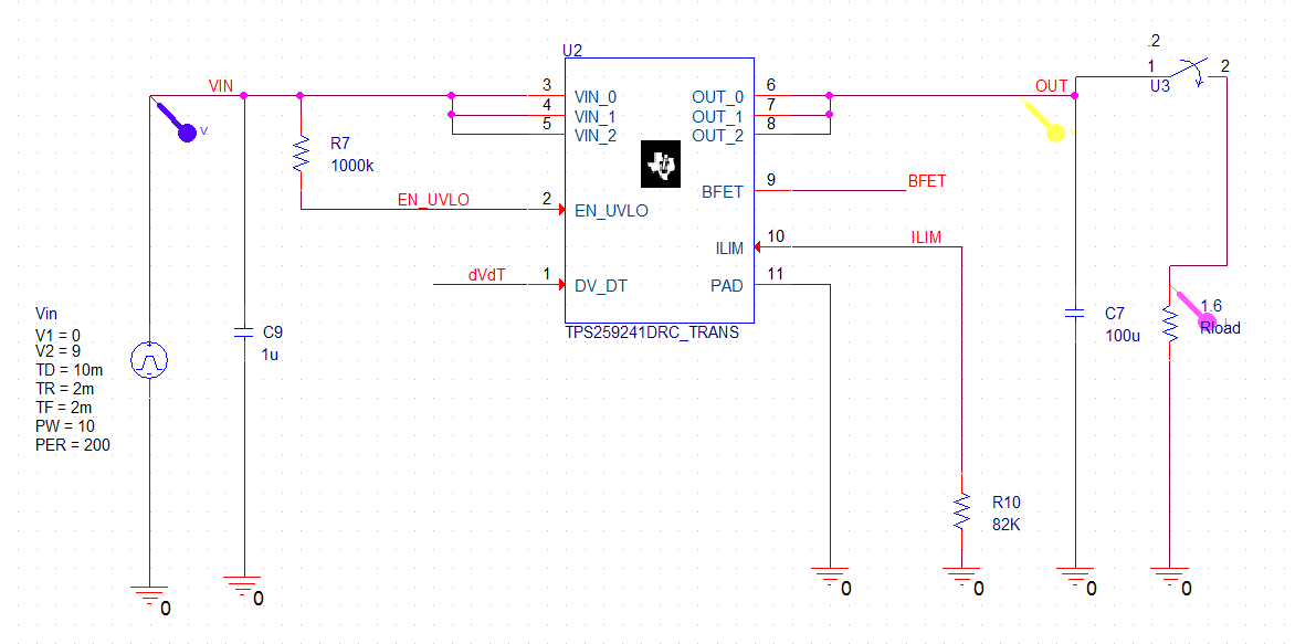
Here's the schematic of the section as we have it designed. Please excuse the part designations not matching the spec sheet, I pulled this off our overall schematic.

Note that CD1 and RZ1 are not used (this is on a PCB, and these pads are left unfilled)

The voltage input is a 9V DC power supply, providing a steady 9V with effectively unlimited current availability.

The desired draw limit is 3.4A.

Using a multimeter, the voltage read at Pin 2 is 8.3V (problem still persists if I connect resistor RS1 to other voltage sources to bring Pin2 to other values). No RZ1 is used because we have no external BFET, we're after a simple max current limiter. 

Regardless of the voltage read/applied to Pin2 (which I understand to be the "enable" pin when pulled HIGH), Pin9 always also reads 0V. I expected it to also go HIGH when Pin2 was enabled, this was interesting to me.

Our load itself is a little non-standard, it's got a variable resistance (it involves some thermoelectric modules, so things get unusual). But, I can't even get this circuit to drive an LED as the load instead.

I've got a suspicion I'm missing some small intricacy regarding the EN/UVLO pin, because otherwise I'm almost a dead match for the example in the spec sheet. Your advice on this would be greatly appreciated!

Thank you!

PS: I've manually pin-to-pin probed our PCBA to ensure that the real-world connections match the schematic-- they do (thankfully). I've also been directly hooking up my loads and sources to test points at the relevant nodes (skipping the other components down the line and isolating the shown schematic)

  • Hi Uzair,

    The schematics looks perfectly fine to me. The only reasons that I can think of why the Output has not ramped up is that either the Load is short circuited or the IC is damaged. have you checked replacing the IC on your board? Have you checked the same circuit on our EVM?
    Can you capture startup waveforms with Vin, Vout, Iin and En ?
  • Thanks for the quick reply!

    Ok, good to know there's nothing apparently wrong with the schematic fundamentally.

    When there is no load, Vout=Vin, correct? 

    My load has a variable resistance, it starts off quite low, and very quickly ramps up. It's possible that the chip sees the large starting current demand (it would be a 7A spike if I hooked it up directly to 9V, decaying to 4A over about 1 second) as a short circuit? But in that situation, Vout should just be reduced until the current demand does not exceed the limit, is that correct? 

    Even so, I've also removed my load and been measuring using no load as well as a small LED to test and getting the same results.

    I haven't used the EVM before, I'll jump into that and try it out! I'll look around the site for it, thanks. I'll also attach some leads to another IC and breadboard it, then replace the one on the PCB. 

    Unfortunately I can't capture proper waveforms with the equipment I've got today, but I'll note the voltages at different stages on those pins (or I'll see if the arduinos I've got around are sufficiently quick and accurate to read off a voltage divider).

  • Hi Uzair,

    What is the total Output Capacitance on the Output rail? Is there only 1uF capacitance? We need to consider the entire capacitance on the rail.
    Your load might have caused a failed startup of the device. Is there a way that you can turn your load ON after Vout ramps to Vin ?
    We will get a better idea if we have the waveforms. Please try the same circuit with your load on EVM. It will be easy to capture waveforms on EVM.
  • Praveen,

    You're right about the capacitance, it's only 1uF. I'll see if changing that solves the problem, that could be it. I'll run simulations to get those waveforms and investigate. 

    I tried using the WEBENCH Power Designer but it said this part wasn't supported. Was that the right software? Could you point me in the right direction?

    The load turns on well after Vin is applied (for my breadboard testing I've got a switch I manually press, and in the application it switches on after several other processes)

    Thank you very much for all your help!

  • Uzair,

    We have Pspice models for TPS25924. You can find them in the below link.
    www.ti.com/.../toolssoftware
    Good to know that the circuit is working fine on your breadboard. So, this indicates that the load in your system in causing a failed startup.
    You can verify this in the simulation as well.
  • Thanks for the links. I'll try running those simulations today.

    I should have clarified-- the load is connected long after Vin is applied, but the chip is still not behaving correctly, and Vo drops out almost instantly. 

    It appears to be related to the current demand of the load, as far as I can tell. When the demand is too high above Ilim, the chip stops conducting (makes sense, the chip must see this high demand as a short). My load consists of two elements-- when only ONE is plugged in (normally a 3.26A demand at 9V), Vo does remain high, and I see a current draw on my power supply of about 2.8A . When both load elements are connected (a 6.18A demand at 9V), the output drops out within a second. On this breadboard I've got an 86Kohm Rlim resistor for now. 

    I've been increasing the load capacitance, all the way up to 300uF, still presents the same problem-- but the shutdown is slower with a larger capacitor. 

    I'll try to run those simulations today to get some more detailed information for you, my apologies for my lack of testing equipment. It seems to be the chip's short circuit response, but I didn't expect Vo to go to zero with a load current about 2x the set Current Limit. Does the dV/dT pin have any effect on this response, perhaps? 

  • Praveen,

    When trying to use the pspice models of the part in both Cadence PSpice and LTSpice I'm unable to get the simulation to run. I see that other users have experienced this too with TI's encrypted models. Is there something I could be doing wrong?

    I tried importing the model into TI-TINA, but I get the "Invalid device: $CDNENCSTART. Line: #56"

    Googling reveals that this means TI has not converted this model into a TINA compatible package. What are my options now? I can't get this simulation working in any other software, and TI's own software (which is quite user friendly compared to the others, I might add) isn't compatible with this part yet.

    I see that in some cases TI has been able to push certain models into the TINA conversion queue. Is this an option here? This part of this project is on halt until I can get this power delivery working properly-- unfortunately I'm without the usual benchtop tools to gather these waveforms so I need to get this simulated. If you believe that this model should simulate properly in LTspice and that I must be doing something wrong, let me know.

    Thank you for your prompt attention on this matter.
  • Uzair,

    Regarding PSpice and TINA models, can you create a seperate thread? I will assign the thread to the correct team so that you get quick reply.
  • Update:

    I was able to get a simulation running in Cadence by using the included Test_Bench file.

    I've been doing a lot of data collection, here's what I'm currently seeing:

    Load Characteristics:

    Measuring amperage with a multimeter.

    Peak Current (direct) represents the current draw for this load when connected directly to a DC power supply. 

    Peak Current (through chip) was measured after Vo on the E-Fuse

    At Rlim=100KOhm, Ilim=3.7A according to Equation (4) on the spec sheet.

    Vin (V) Peak Current (direct) (A) Equivalent Resistance (Ohm) Peak Current (Through Chip) (A) Rlim (KOhm) Condition
    10 6.29 1.59 4.886 100 FAILS (Vo falls to 0)
    9 5.793 1.55 4.507 100 RUNS
    8 4.991 1.6 3.847 100 RUNS
    7 4.322 1.62 3.517 100 RUNS
    6 3.792 1.58 3.037 100 RUNS


    At Rlim=82KOhm, Ilim=3.16A

    Vin (V) Peak Current (direct) (A) Equivalent Resistance (Ohm) Peak Current (Through Chip) (A) Rlim (KOhm) Condition
    10 6.29 1.59 2.626 82 FAIL
    9 5.793 1.55 4.195 82 FAIL
    8 4.991 1.6 4.061 82 RUNS
    7 4.322 1.62 3.472 82 RUNS
    6 3.792 1.58 2.998 82 RUNS

    It appears that at current demands that exceed the current limit by too much, voltage output drops to 0. This doesn't seem to match what I was expecting-- the spec sheet even shows a waveform of an output short, and even then the output doesn't completely drop to 0. 

    I also see that output currents exceed the set current limit-- why is this? The multimeters I'm using are recently calibrated, and these measurements occur across multiple meters. I've listed peak currents in the tables, but even subsequent steady state current is above Ilim for quite some time, several seconds. In the spec sheet I see that even in the event of an output short, Vo is only reduced such that the output limit is met. This doesn't seem to be behaving in that manner on my breadboard. 

    Simulation Results:

    I ran the simulations, using a 1.6Ohm resisitor as the load. I've got  a switch (U3) that closes at 200ms to "turn on" the load separately from the Vin startup.  I see what looks almost like a pulse-width output on these waveforms, also not what I expected. In the case of my actual circuit, this also is not the exhibited behavior-- the voltage Vo does not come back up after dropping out. 

    My actual load is a thermoelectric module, for which I cannot find a pspice model, so I used a resistor here instead. 

    In order to make a waveform that mimics the behavior I'm expecting, I changed the Rload to 2.6ohms, and got the following, which is in line with what I'd expect to see:

    So, a few questions:

    Why is my real-world output dropping to 0 when the amperage demand is beyond a certain level too high? In some cases, the chip appears to throttle the output (although not all the way down to Ilim), but in other cases it throttles and fails.

    Why is the conducted current greater than Ilim in certain cases? 

    What's the reason behind the differences in the waveforms between Rload=1.6 and Rload=2.6? Why does a higher current demand (lower Rload) then result in this pulse-width-like format? 

    Vin (V) Peak Current (direct) (A) Equivalent Resistance (Ohm) Peak Current (Through Chip) (A) Rlim (kOhm) Condition
    10 6.29 1.59 4.886 100
    9 5.793 1.55
    8 4.991 1.6
    7 4.322 1.62
    6 3.792 1.58
  • Hi Uzair,

    Thanks for sharing your test results. Please see my response below for your queries,

    • During an over current event, the load current will be limited to the value programmed by RILIM. There is a tolerance for the current limit as shown below. Please measure the steady state current during current limit  rather than the peak current. Also please consider the tolerance of the RILIM resistor that you have used. 
    • The short circuit waveform in datasheet shows Vout=0.


    • Let us consider that you have selected RILIM=82k. This makes the ILIM 3.1A. Consider Vin= 9V.
      • Now, when you connect a load of 1.6 Ohms, the current that should be flowing in the FET before it starts to current limit is 9/1.6 = 5.62 A. As this current is greater than ILIM, the device limits the current to 3.1A. To achieve this the FET resistance is increased. If you calculate the FET resistance has to be 1.3 Ohms to limit the current to 3.1A (9V/3.1A = 2.9 Ohms, 2.9Ohms - 1.6 Ohms = 1.3Ohms). 

                   The voltage drop across the FET would be 3.1A x 1.3 Ohms = 4V. This means Vout = 5V (9V - 4V).

          Now, the power loss in the FET would be 3.1A x 3.1A x 1.3 Ohms = 12.49W. Considering a 35 C/W of thermal resistance, temperature rise over            ambient would be 12.49 W x 35 C/W = 437.255 C which is way above the thermal shutdown threshold of 150C. So, the IC shut down. Since you            are using TPS259241  which is an Auto retry part, the FET tries to turn ON once the temperature falls 10C below 150C. 

      • Now, when you connect a load of 2.6 Ohms, the current that should be flowing in the FET before it starts to current limit is 9/2.6 = 3.46 A. As this current is greater than ILIM, the device limits the current to 3.1A. To achieve this the FET resistance is increased. If you calculate the FET resistance has to be 0.3 Ohms to limit the current to 3.1A (9V/3.46A = 2.6 Ohms, 2.9Ohms - 2.6 Ohms = 0.3Ohms).

          The voltage drop across the FET would be 3.1A x 0.3 Ohms = 0.93V. This means Vout = 8.1V (9V - 0.93V).

          Now, the power loss in the FET would be 3.1A x 3.1A x 0.3 Ohms = 2.88W. Considering a 35 C/W of thermal resistance, temperature rise over              ambient would be 2.88 W x 35 C/W =  100 C. Adding Ambient temperature of 25C, the total junction temperature is 125C  which is below the                  thermal shutdown threshold of 150C. So, the IC wouldn't shut down. 

    The calculations are inline with what you see in the simulation.

    So, Vout is dependent on the drop in the FET which is dependent on Vin and Load.

    The shut down of the FET is dependent on the internal FET junction temperature which is dependent on the power loss in the FET. 

    Hope, I answered your questions.  

  • Praveen,

    Thank you so much! This was extremely helpful-- you clarified all of my misunderstandings, and I clearly see what's going on now. I had made some incorrect assumptions before, this is one of my first in-depth  electronic projects, and this helps me understand quite a lot. 

    Have a nice day, thanks again

    -Uzair