This thread has been locked.

If you have a related question, please click the "Ask a related question" button in the top right corner. The newly created question will be automatically linked to this question.

LM5085: Dead MOSFET after 48V application

Part Number: LM5085
Other Parts Discussed in Thread: LM5146, LM5145

Hey E2E,

I am using the LM5085 in a 48V -> 12V @ 10A application. I am using a Webench design which has been slightly modified to fit my spec. (Webench schematic can be found here)

Vin: 48 - 55V

Vout: 12V (+-.2V)

Iout: 10A (roughly)

I was able to create a crude prototype on a breadboard using an SMT breakout PCB that was able to output 12V from 55V with no issues. I then put the design onto a PCB and manufactured it. After trying to test it with 48V however, I only saw 48V on the output (this was a no-load condition). After probing around the board the P MOSFET was discovered to be dead (Gate, Drain, and Source were all shorted to each other). I'm not sure what could have caused this. I replaced the MOSFET to see if that would fix the issue (could be just bad luck), but the issue persisted.

Some other notes: I tried applying 15V just to see if it was a fatal design flaw at all voltages but the board was able to output 2.4V (meaning at least something was getting converted). No load was shown to be drawn at this voltage (meaning it's not an internal short anywhere). It also appears to not have affected any other component on the board (diodes, inductor, LM5085, and anything else on the current loop seem to be fine). Finally, I did not put as much capacitance on the output/input side of the board as stated in the schematic. My thought was that more capacitors could be added on once I started doing load tests.

My guess is something is wrong with my choice of MOSFET, the SUD50P08-25L, but the specs on this indicate it should be fine for this application (-80V VDS max, +-20V VGS max). Below are my schematics as well as the board layout.

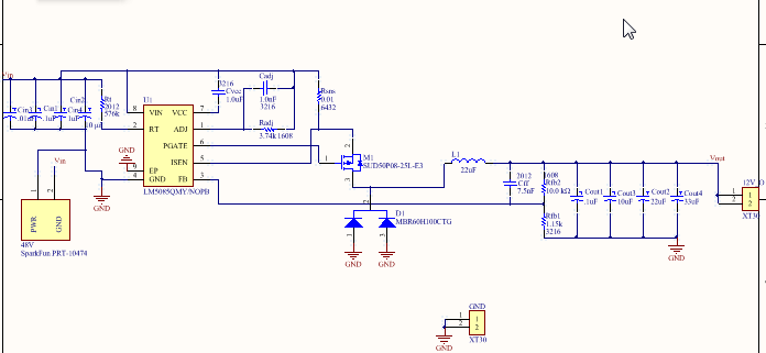
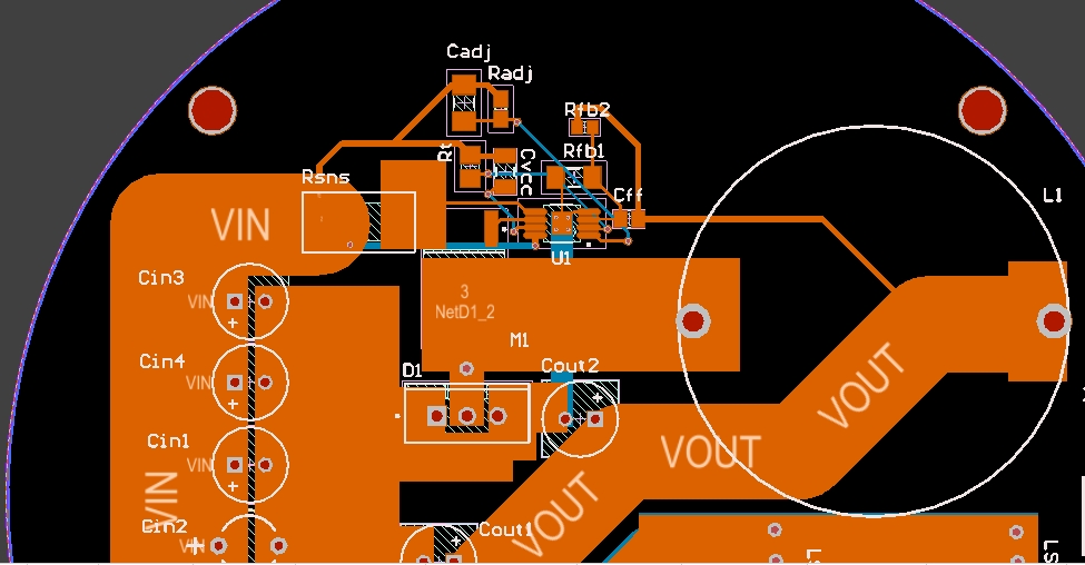
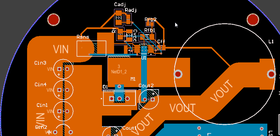
The connectors are cut off from the PCB views, but they aren't relevant to the problem (just XT60/XT30 connectors). The project is also available on CircuitMaker if an in depth view is needed. 

Any help/guidance is appreciated,

Thanks!

  • At what Vin does the FET become damaged?
    Do you get the correct output at VIn = 24V or other lower input?
    Can you probe the gate and drain node of the FET when it is running.

    There may be some things in the layout that may cause this.
    1. The small value input bypass cap must be close to the device VIN and GND pins.
    2. In general I would beef-up the traces going to the VIN and GND of the device
    3. The feedback for Vout should be made near the output capacitors.
  • Hey Frank,

    Thanks for replying so quickly. I replaced the FET on the board and the LM5085 (just in case) and tried powering on from 0 - 30V (programmable supplies we have around here only go to 30V, the 48V supply I used before is just a static supply). I also learned that the capacitors used for Cadj and Cvcc were only rated to 50V max. The supply I used before can go up to 55V (on startup) on VIN so I believe that may have been the source of my issues. I replaced those with new ones and went ahead with the lower voltage testing.

    The measured output scaled up from around 0-2V Vout @ 0 - 20V Vin and then from 2 - 12.12V Vout @ 20 - 30V Vin.  At 30V the output appears to be normal. (*note: these are all no-load conditions).

    When I applied a probe (1M impedance) to the Drain (+) and Gate (-) of the FET I saw the below waveform. The output (Vout of the whole device) showed some really odd results, the voltage was a constant 3V below the input (so at 5V vin, it was ~2V vout and at 30V is was ~27V). Not sure if that's supposed to be normal behavior... When the probe was removed, the output returned to the aforementioned behavior (30V in -> ~12.12V out)

    Throughout this whole process, the FET remained functional. I'm going to purchase some new caps (ones that are rated for 100V+) and see if that solves my problem and I'll make an update with my results. In the meantime, here are the waveforms, just in case the caps aren't my issue and there's still something going on. 

    Below is V (drain -> gate) at different inputs

    Vin = 5V

    Vin = 8V

    Vin = 15V

    Vin = 30V

    Thanks!

  • It looks like the switching is rather slow, if the scope is set to 10ms/div.
    If you have a chance you might want to make some of the suggested layout changes.
  • I am closing this due to inactivity.
  • Hey Frank,

    Just wanted to follow up, sorry for the long delay.

    Got the parts in 2 days ago and made up another board. This one showed similar behavior to the others before it so unfortunately the issue isn't resolved.

    In a bit of experimentation I tried putting on a different FET (STP12PF06) to see if that made any difference. I just soldered on some jumper wires (The package was TO-220 vs the DPack I was using) and put them onto the pads of the board after taking off the original FET. Crazy thing is, the board then started outputting the correct voltage at no load and all the way up to 1.5A. After which the voltage went to 0 (could be a current sense issue there). I then tried soldering the new FET on directly and suddenly the board stopped working (started behaving erratically, similar to before).

    I'm now completely lost as to what the issue could be. Is there some small impedance necessary to the Gate/Drain/Source side of the FET that I'm not aware of? I can get any necessary waveforms, I'd just really like to get this thing solved.

    Thanks
  • I will try to find one of our EVMs and send it to you. You may be able
    to use it to get a working design.
  • I spoke with the application engineer for this device.
    This device may not be the best choice for you application.
    He has suggested the LM5145 or the LM5146.
    You could use the LM5146 EVM as a starting point.
  • I am closing this due to inactivity.