This thread has been locked.

If you have a related question, please click the "Ask a related question" button in the top right corner. The newly created question will be automatically linked to this question.

BQ76930: CHG Mosfet Driver for BQ76930/76940

Part Number: BQ76930
Other Parts Discussed in Thread: TIDA-01093


Hello.

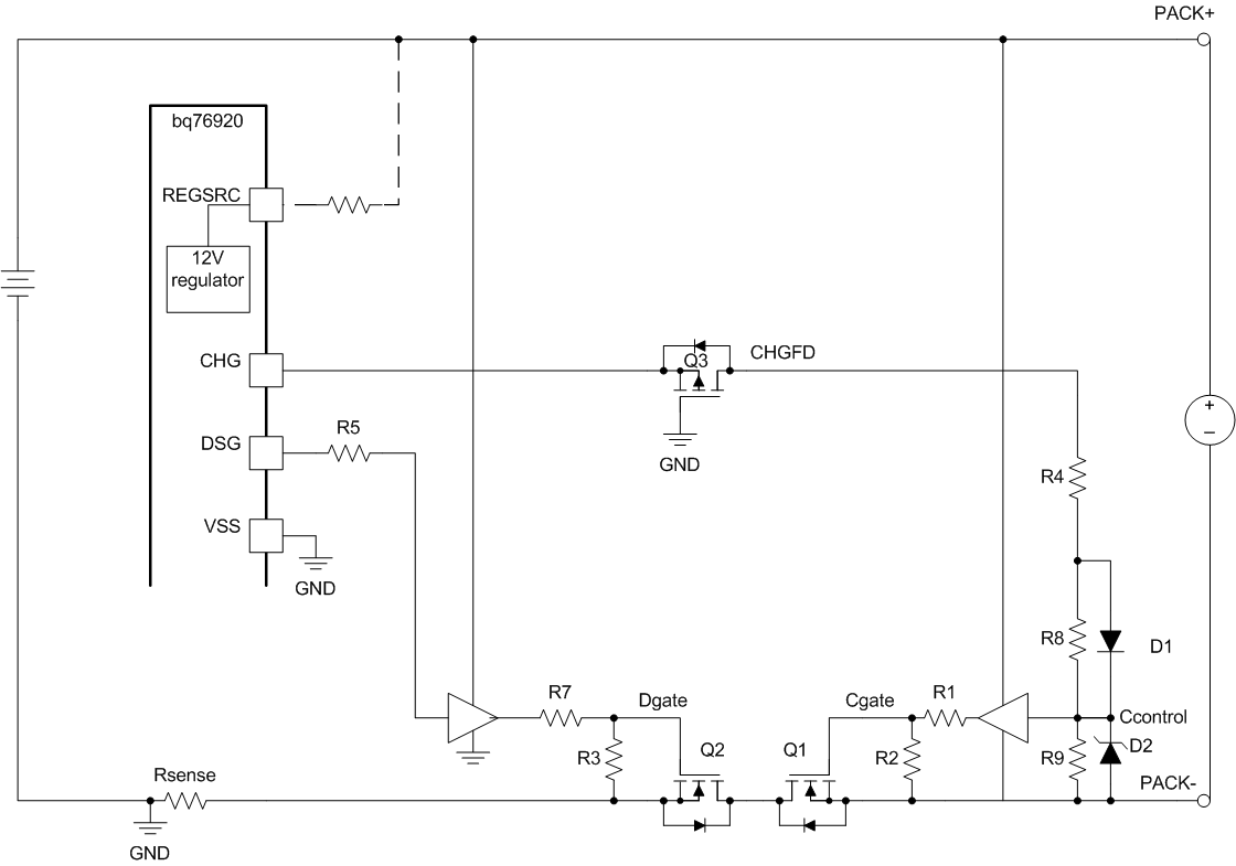
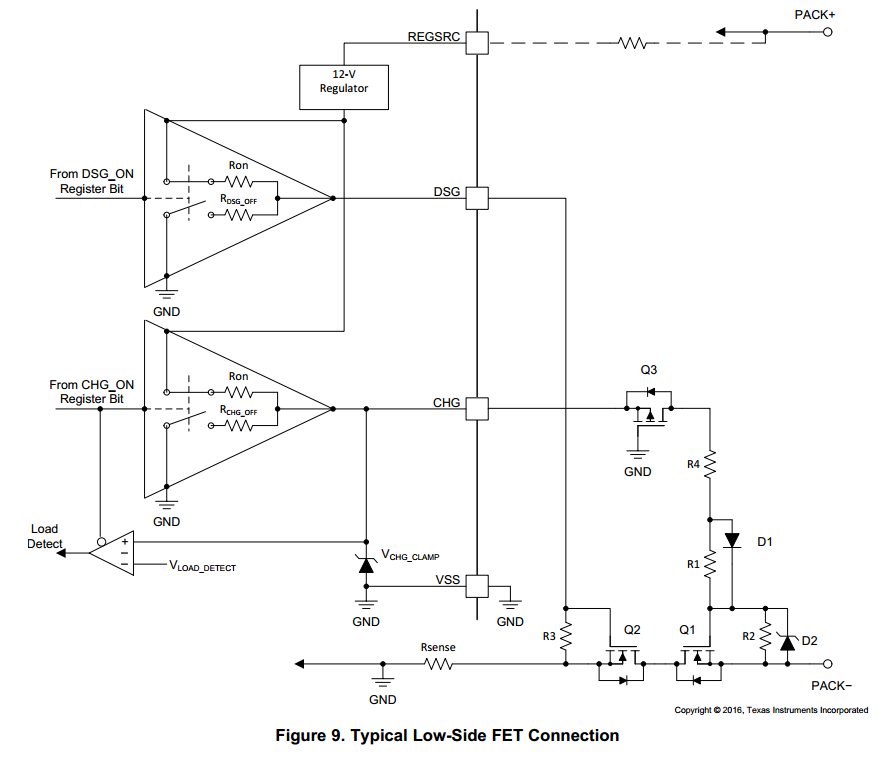
1.I have a question about the CHG mosfet(Q1) drive,in the figure 9 we can see that the chg FET drive circuit  take "GND" reference for grante,the chg output connect to the gate of Q1,when without external load,the source of Q1 is floating, i think because of  the source of Q1 and the chg FET drive circuit not reference for a same grante,the Cgc  capacitance of Q1 has no charging loop,so Q1 can not be turn on.Who can tell me the working principle about  this circuit?

2.Is there any MOSFET drive IC used for BMS low side mosfet?bq76930 drivecapability is not  enough.

  • Hi User,
    Yes, CHG turn off is high resistance and once CHG gets to the Q1 and/or Q3 turn off point it is R2 acting on the Cg which completes Q1 turn off.
    1. If PACK- is high impedance and both Q1 and Q2 are off, there is no DC current path to turn on Q1. When CHG goes high Q3 turns on and R4 and R1 bias the gate at the CHG voltage. R2 biases the PACK- at the CHG voltage.
    If Q2 is on (DSG turned on before CHG), the Q1 body diode holds down the source and the gate voltage can rise with CHG voltage so Q1 turns on.
    If PACK- is held up by a load, the load biases the source of Q1 up, and through D2 the gate also. Current is limited into the CHG pin by R1, R4 is small so has little effect, Q3 is on, CHG may be pulled up higher than its output level.
    If PACK- is driven to a voltage at or below BAT- (GND in the diagram) by a charger, when CHG goes high the charger holds PACK- low while CHG goes up turning on Q1 and pulling (GND) and PACK- together.
    2. Many FET drivers are designed to drive MOSFETs fast for switching power supplies. A challenge using a driver for Q1 is that its supply must float with PACK-. The added supply current of a regulator and driver in a battery may be undesired. A circuit can be used to provide an increased pull down on the charge gate. One solution could be to invert the CHG signal and use it to clamp the Q1 gate low when desired. Another may be to use a depletion mode device to clamp the Q1 gate low. Another would be to use a latch like circuit such as in TIDA-01093 (Q35, Q36 & related). Another is to use a transistor to add gate load such as Q9 in figure 6 of www.ti.com/.../slua773.pdf .
  • Thanks for your replay.
    1.If PACK- is high impedance and both Q1 and Q2 are off, there is no DC current path to turn on Q1. When CHG goes high Q3 turns on and R4 and R1 bias the gate at the CHG voltage. R2 biases the PACK- at the CHG voltage. That is,in this condition,even if CHG goes high,Cgs capacitance of Q1 has no charging loop,Q1 will keep off? If there is a load on pack+ and pack-,Q2 is off, Q1 can be turn on?

    2.If Q2 is on (DSG turned on before CHG), the Q1 body diode holds down the source and the gate voltage can rise with CHG voltage so Q1 turns on.This condition is apply to PACK discharging.So,when the pack discharging,it would be turn on Q2 first and then turn on Q1?

    3.If PACK- is held up by a load,CHG may be pulled up higher than its output level.In this condition,when CHG goes high,Q1 can be turn on?

    4.If PACK- is driven to a voltage at or below BAT- (GND in the diagram) by a charger,In this condition,because Q2 has not turned on,PACK- and GND not connect together, the source of Q1 and the chg FET drive circuit not reference for a same grante.Cgs capacitance of Q1 also has no charging loop,why Q1 can be turn on by CHG?

    5.A challenge using a driver for Q1 is that its supply must float with PACK-. But driver for Q1 in bq76930 take "GND" reference for grante.What's the disadvantage to this approach?

    Looking forward to your reply.
  • Hi User,

    1. With PACK- pulled up, the Q1 FET can not turn on.

    2. If Q2 turns on it will pull down PACK- gate. It will pull down the body diode of Q1. If CHG is on Q1 will turn on.

    3. If PACK- is held up by a load, CHG low or CHG high will not make a difference, the gate will be below the source and the FET will stay off.

    4. The source of Q1 (PACK-) would have a reference by whatever is pulling PACK- low. It will provide a loop.

    5. In this diagram the supply for the driver is shown going to BAT+ Most drivers will have a more limited voltage range which will require a regulator. It is a lot of circuitry which takes space, current, and has cost.