This thread has been locked.

If you have a related question, please click the "Ask a related question" button in the top right corner. The newly created question will be automatically linked to this question.

UCC27714: UCC27714 damages the switches in SPWM code

Part Number: UCC27714
Other Parts Discussed in Thread: UCC27712

Hi,

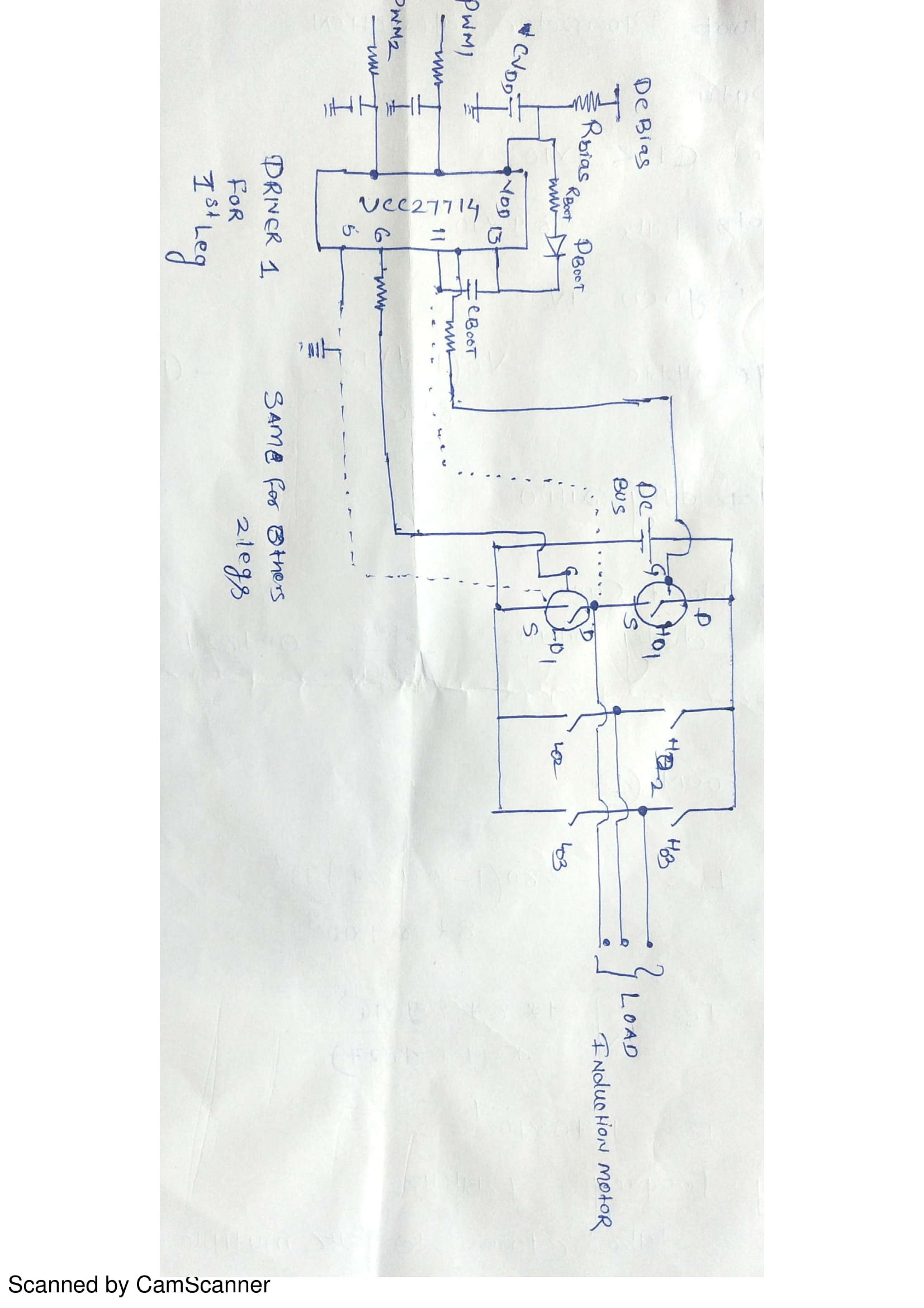
I am using UCC27714 driver circuit for my 6 switch INVERTER. When i tested it with simple 180 degree Square wave inverter with induction motor load it is working fine.

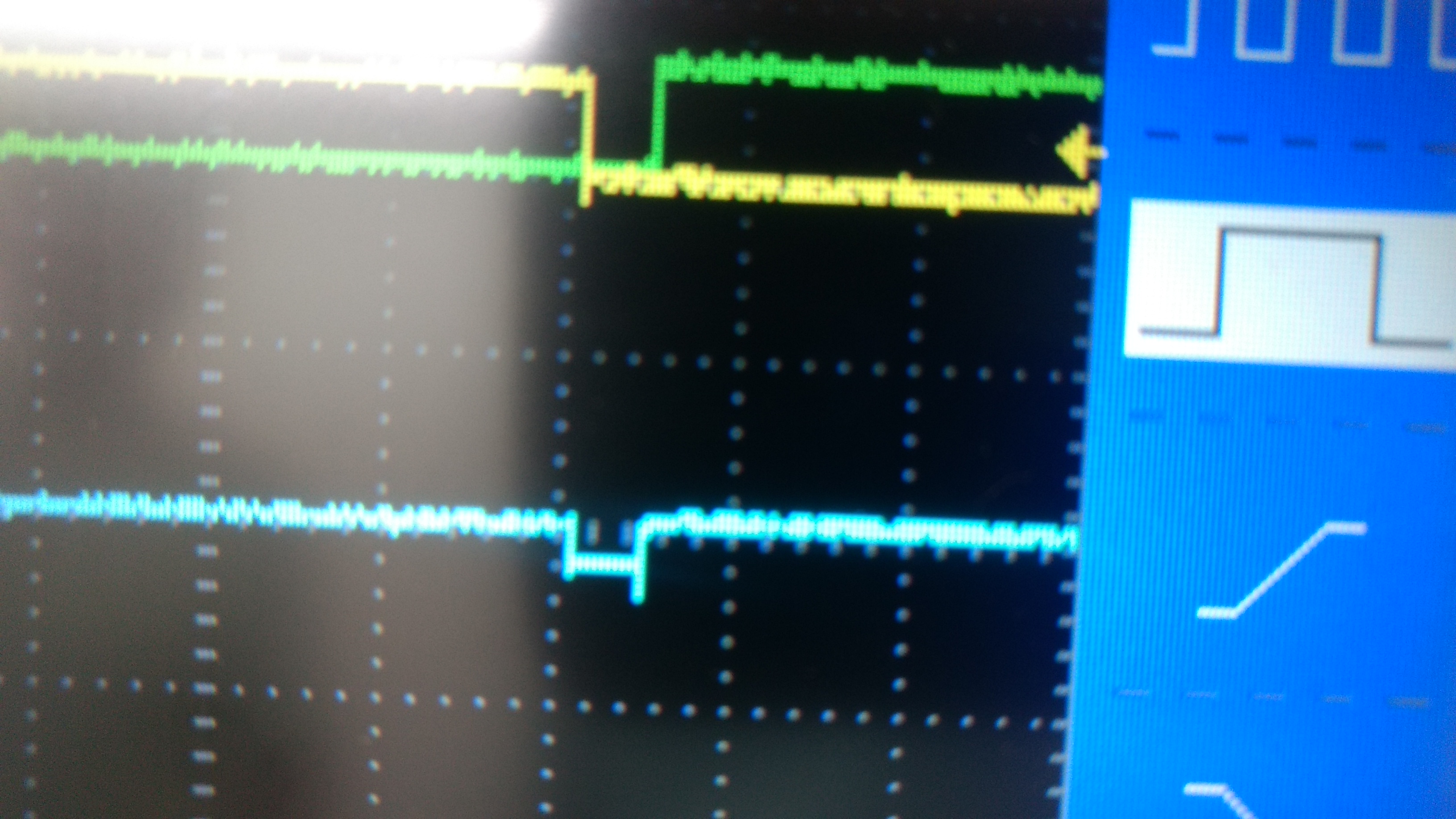
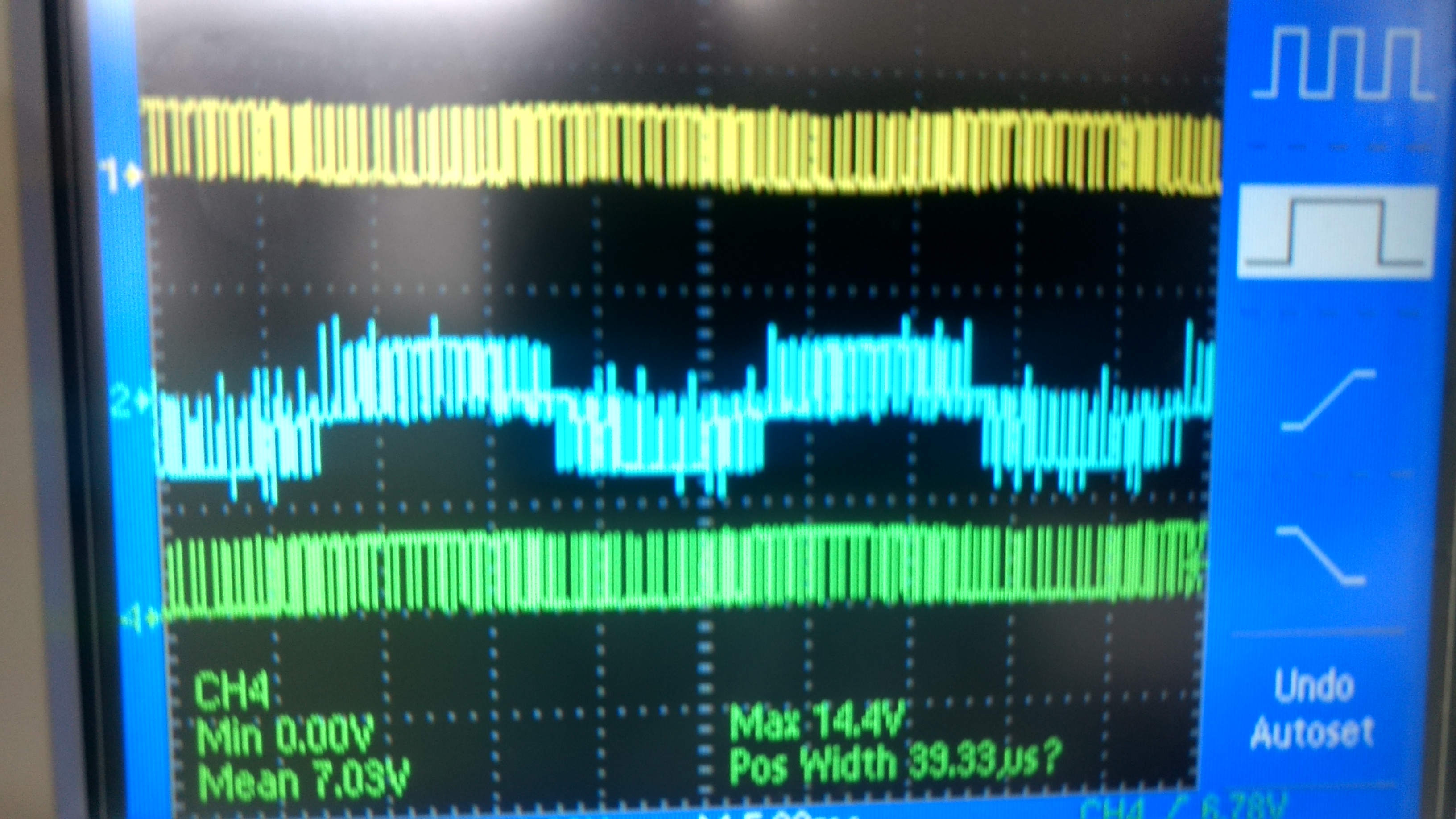
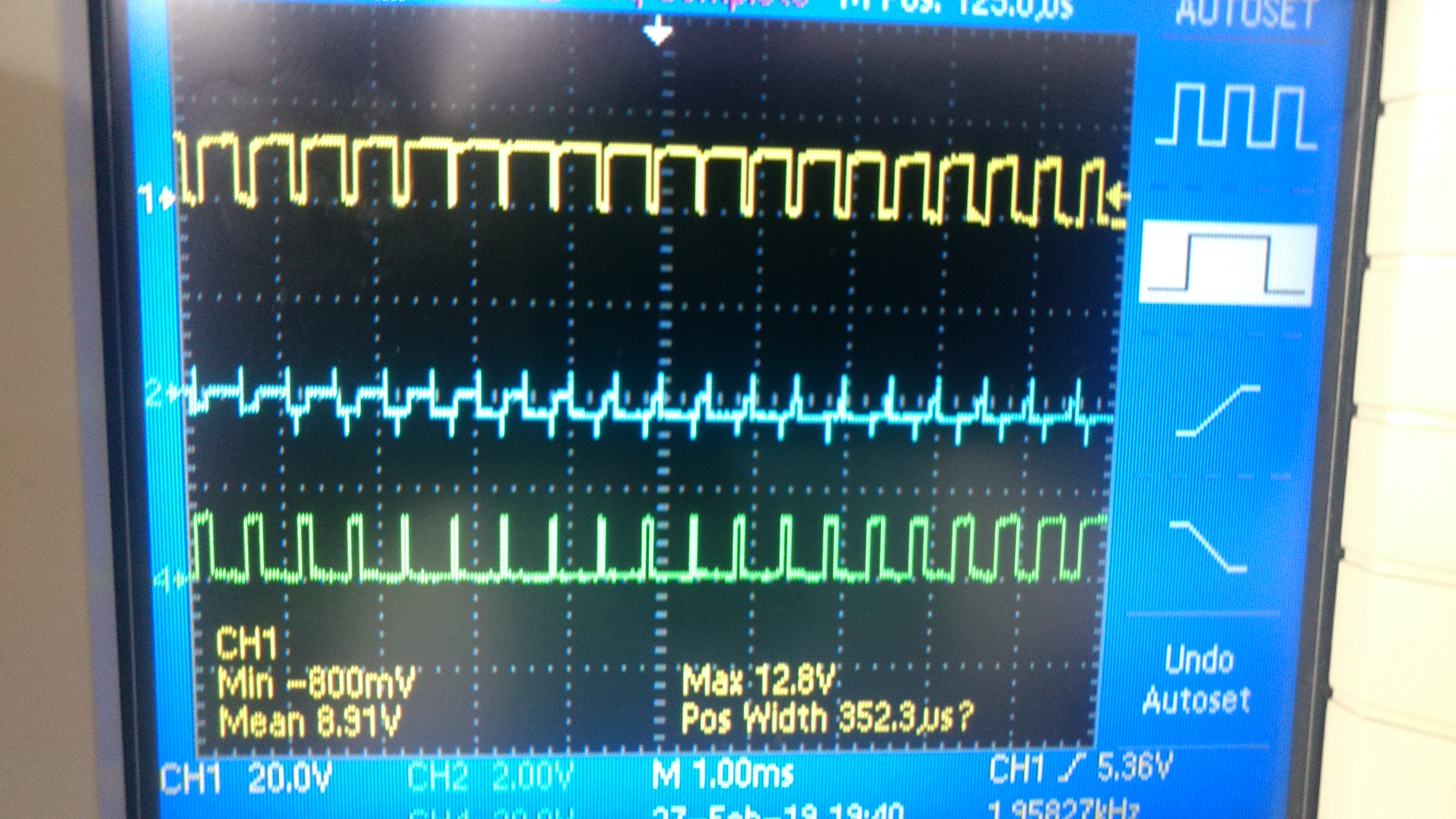
But when i am loading SPWM code with 2khz switching frequency it damages all the switches. I test the same code with other driver circuit  it is working fine.

Please suggest me the solution. because it simply damage the switches at no load conditions also.

but for 180 degree square wave it is working fine for induction motor and others loads also. but for SPWM  and SVPWM with 2 khz it is not working at all.

pwm pulses coming but after applying dc voltage it damages the switches.

I check the dead band also and from code side it is 3 micro second which fine according to switch

  • Hello Ashwani,
    Thank you for the interest in the UCC27714, I support this device and will work to support your concerns.
    I want to make sure I understand the operating mode and conditions, of the square wave inverter mode, and the SPWM mode.
    For the square wave inverter mode, is this 2Khz square wave with high side then low side in constant on time? I assume this is driving the half bridge with a square wave with some dead time from high side to low side power switch drive.
    For the SPWM mode, is the effective sin wave frequency 2KHz with the pwm operating at a higher frequency? What is the PWM frequency?
    Can you provide a schematic of at least the driver, driver support components and power switch circuit?
    Also do you have any scope plots of the operation, at least in the working square wave inverter mode?
    There are a number of things which may cause the driver not to function as expected, I will need to get some information to be able to determine what may be the cause.
    One question, regarding the other driver you mention that does not have the issue. Is the driver current rating the same 4A/4A as the UCC27714? If the drive strength is less, there will be lower dV/dt on the power devices which may be the difference.
    You can try increasing the resistance from the driver to the power switch gate to reduce the dV/dt which may help the issue.
    You can post additional questions or information on this thread.

    Regards,
    Richard Herring
  •  Dear Rechard,

    Thanks for reply , I am clearing you confusion first. The square waveform frequency is 50 Hz fundamentally. and it switch also according to that. We are operating in 180 degree mode and the wave forms are inserted .We are getting exactly same waveform while driving Induction motor in square wave operation mode.

    Next in SPWM or SVPWM sine wave forms are again 50 hz only ,

     but pwm switching frequency is at 2 kHZ with dead band about 3 micro seconds.

    i am using switches FCH125N65S3R0,of 24 Amps and 600V ,but driver damages it at no load also.

    I am attaching the schematic of switches along with driver circuit. 10K resister connected at output we removed because it creates the problem in square wave also.

    Same schematic runs perfectly for square wave operations but when i apply higher switching it simply damages the switches.

  • Dear Rechard,
    please can you solve the issue..i already given you the information which you asked
  • Hello Ashwani,

    Thank you for the information on the operating details and the basic schematic of the driver and power MOSFET circuit.

    Since you are operating a low frequency, you should confirm if the bootstrap capacitor and VDD capacitor are sized properly.

    For design guidance in low frequency applications refer to the similar gate driver datasheet UCC27712 Section 8.2. Cboot suggested value is determined by the following.

    Determine Qtotal based on MOSFET Qg, switching frequency, and UCC27714 Iqbs. Iqbs is the HB-HS quiescent current. Qtotal=Qg + Iqbs/fsw. For 2kHz: Qtotal= 46nC + 120uA/2kHz= 109nC. For 50Hz: Qtotal=46nC +120uA/50= 2446nC.

    Determine Cboot from: Cboot=Qtotal/deltaVboot. I am going to assume VDD is 12V, please confirm, and we will target 10V minimum VHB for the MOSFET drive. This will result in 12V-10V-0.7V (boot diode Vf)=1.3V allowable delta V. Cboot=2446nC/1.3V = 1.88uF for 50Hz, for 2khz: Cboot=109nC/1.3V = 83nC minimum.

    The VDD capacitor is recommended to be 10x the Cboot, or 22uF for 2.2uF Cboot. We also recommend a higher frequency bypass capacitor such as 100nF in parallel.

    For Rboot we recommend a range of 2.2 to 20 Ohms for Rboot. Since Cboot is relatively large I would suggest an initial value of 2.2 Ohms, and insure that the boot diode peak current rating is higher than VDD/Rboot.

    For Dboot select a fast recovery diode to minimize charge being removed from Cboot when HS switches high. Select a 25-50ns recovery diode such as the MURS160.

    Can you confirm the component values you are using in the application: CVDD, Cboot, gate resistance, Rboot, and boot diode part number?

    Also do you have the resistor and capacitor bypass on the HI and LI pins? If so these values will be helpful to review.

    Failures of the driver can occur for a number of reasons: voltage overshoot or undershoot on the LO and HO pins, overvoltage of HB due to HS negative undershoot, ringing or noise causing false triggering of the driver outputs.

    Can you provide the gate driver output scope waveforms, operating in a working condition? 50Hz square wave. SPWM with HV not applied, or lower level. Provide scope plots of LO, HO, HS, and HB. It is best to see HO-HS measured with a differential probe. Zoom on a time scale to see the turn on and turn off waveform details.

    Regards,

    Richard Herring

  • Hello Richard Herring,

    thanks for replying but my issues are not resolved.

    I am sending you complete design which i used for two different switches with  switch  part Name ...as suggested by you but in both the cases after certain voltage switches were damaged

    .For Switch FCH125N65S3R0.

    My design Parameters are as follows. for 2 kHZ frequency

    Rbias =5 ohm

    Cvdd = 1uf

    Cboot= 0.1uf

    Rboot =3ohm

    Dboot MURS16013F

    RLI =RHi = 47ohm

    CLI =Chi = 220pf

    RLo = Rho = 3ohm

    For Switch IRFP450 @ 2KHz

    Cboot = 0.2Uf

    Cvdd = 2 uf

    rest all components are same

    Now i am sending the snaps of scopes you will observe that we are getting glitches in Dc bus voltage because of Switching and that may damages the switches.

    in first figure

    Blue line indicate Dc bus voltage which is Zero but due to switching instant it shows glitch. Above are gate pulses with dead band.

    In fig 2 same blue color shows line voltage which is again with lot of disturbances rest green and yellow are gate pulses.

    In last figure also blue is Dc bus voltage  which is 0 volts but due to switching glitches are coming.

    i designed exactly the values given by you but still

    simply it damages my switches.

    Note: This all design is working if i designed according to 50 hz .its working fine on induction motor load also

  • Hello Ashwani,
    Thank you for the design component values. The Boot diode, boot resistance, and bias resistance look OK. The CVDD and CHB capacitance looks OK for the 2kHz operation, but for the 50Hz I am not sure how the VHB can be sustained. During 50Hz operation is the high side on for 1/6 of the period, or 3.3ms? That will make a difference.
    The dead time shown in the top plot should ensure enough time for the devices to turn off before the opposing switch turns on.
    Since you have trouble operating high voltage applied to the power train, and ability to capture these waveforms, I will have to make some suggestions based on what may happening to create issues.
    I see the gate resistor is 3 Ohms which with the smaller FET will result in a rising time constant of 13ns. With this low frequency operation you should be able to switch at lower speed without too much impact on loss.
    If you look at the MOSFET datasheet you will see that the body diode recovery time of high voltage MOSFETs is long, The two MOSFET's you mention is 339ns to 540ns body diode trr. I am not totally familiar with the detail power train waveforms of the sin wave inverter, but if there is continuous current flowing during switching, which results in body diode conduction of the opposing switch, when you turn on the MOSFET there will be a high current path thru the turned on switch and opposing switch body diode until the diode turns off.
    In this case, there can be high dI/dt and resulting high voltage spikes and ringing from this high current when the body diode turns off.
    Increasing the turn on gate resistance is the most common method to limit these voltage spikes.
    I would recommend increasing the gate resistance for turn on to higher values starting with 10 Ohms, and higher to see if this helps.
    It is possible these conditions exist operating in SPWM mode but not in the 50Hz mode.
    If there is high voltage spikes on the half bridge switch node, in some cases the miller capacitance can couple enough energy into the gate terminal to result in voltage overshoot and undershoot on the driver output pins. If these spikes exceed the rating the driver can be damaged or malfunction. To address this issue, place 1A 20-30V scottky diodes from the driver output to VDD and COM for LO, and HB and HS for HO. Place as close as possible to the driver.

    Let me know if any of this advice helps, if you are able to achieve operation with HV applied, but still have some remaining issues please provide scope plots of the waveforms.

    Regards,
    Richard Herring