This thread has been locked.

If you have a related question, please click the "Ask a related question" button in the top right corner. The newly created question will be automatically linked to this question.

UCC27712: Ringing - Gate Drive or Switch Node?

Part Number: UCC27712
Other Parts Discussed in Thread: UCC27714

Hello,

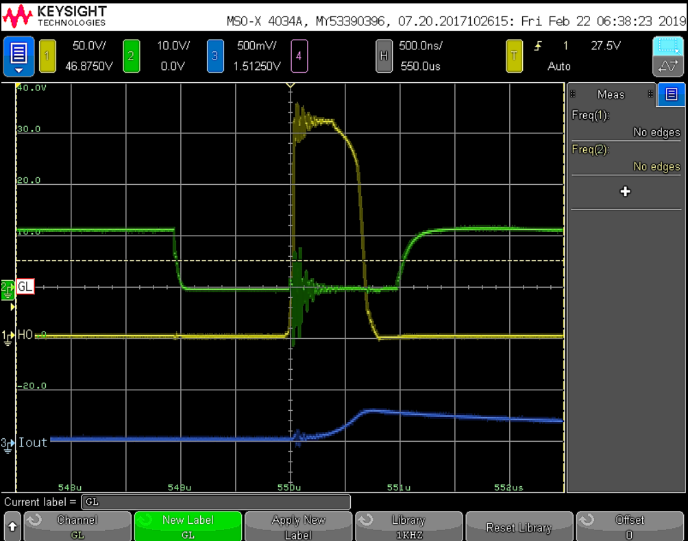
Looking at these waveforms, does the ringing look like it is originating from the gate drive? Or is the ringing is actually on the switch node? (First Picture)

My thought is that the ringing is truly on the switch node, because we can see the ringing coupled onto both the high and low gate drive signals. (Second Picture)

However, I am curious if maybe it is the high side gate drive that is ringing, thus causing the switch node to ring as the FET's Rds(on) changes.

  1. If the ringing is from the gate drive, is the solution to simply increase the gate resistor?
      1.  
  2. If the ringing is from the switch node, what values can I change to help?
      1.  

This is on the EVM, so I'm not concerned about layout. However, we did change the gate resistors to 2.7-Ohm. On the switch node is a large inductor, value between 2.5mH - 10mH don't seem to help the ringing.

Thank you!
Ryan B.

  • Hello Ryan,

    Thank you for the interest in the UCC27714. The ringing in the 1st plot is showing ringing on the switch node and HO output relative to ground as you mention.

    The HO output is referenced to the HS pin or switch node so the actual gate drive and Vgs waveform will be the differential measurement of HO-HS. There is typically some voltage spikes and ringing on the switch node which is the result of switching edge dV/dt and dI/dt and the parasitic inductance and capacitance of the layout and MOSFETs. Typically ringing on the MOSFET Vgs is not the source of the switch node ringing, but Vgs ringing can slow down the switching edge process. If the Vgs ringing is excessive it may cause the MOSFET to switch unexpectedly but that does not appear to be the case in these plots.

    The switch node ringing can be reduced by a couple of methods. Slow down the switching edge dV/dt by increasing the gate resistance. Adding snubber to the switch node to dampen the ringing.

    Confirm if this answers your questions, or you can post additional questions on this thread.

    Regards,

    Richard Herring