hello, i just started to grow interest in electronic and trying to design a pcb using LP5912-3.3DRVR as my 3.3v LDO. sorry if my questions might be very simple but i lack knowledge in some areas. i have 3 diagrams please take a look at them.
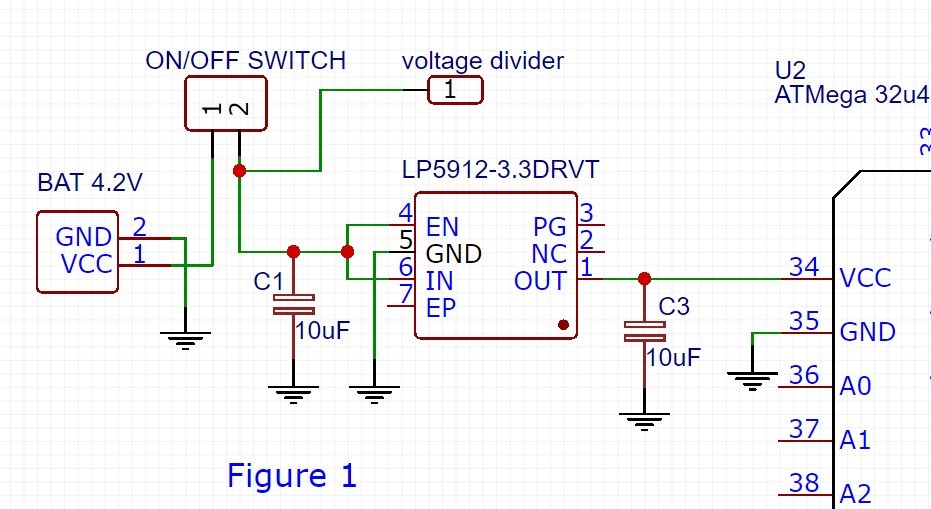
1-in this figure 1 im trying to feed that microcontroller on the right and the datasheet of it advises for a 10uF cap to be placed between vcc and gnd pins. LP5912 will be placed next to that microcontroller so can they share that 10uF (C3) cap or i should add another one?
2-if you noticed i added external mechanical switch to vcc line(from BAT) which goes to IN of LP5912 because i also want to cut power of that voltage divider. i seen in the datasheep that PG pin can be left floating or connected to ground but couldnt find anything about EN pin. most other LDOs tell you that you can connect it directly to IN side if you dont need EN function. so does that also looks correct?
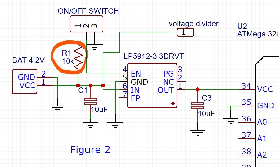
3- if i ever decide to use EN function does that look ok? i have seen some other examples using a resistor(10k- 100k) between the IN and EN pin do i need it here or should i remove it?
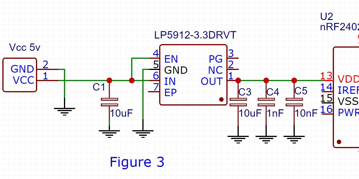
4- this is my second application and the chip that im trying to feed suggest to use 3rd cap(C3) in range of 4.7uF-10uF in addition to 1nF(C4) and 10nF(C5). i have noticed in the datasheet maximum output capacitance should be 10uF. so in this application can i keep it as it is or should i reduce that C3 to 4.7 uF?
thank you for assistance have a nice day.


