Other Parts Discussed in Thread: SEGGER
We have produced a new batch of boards and see this problem ~1% of the time.
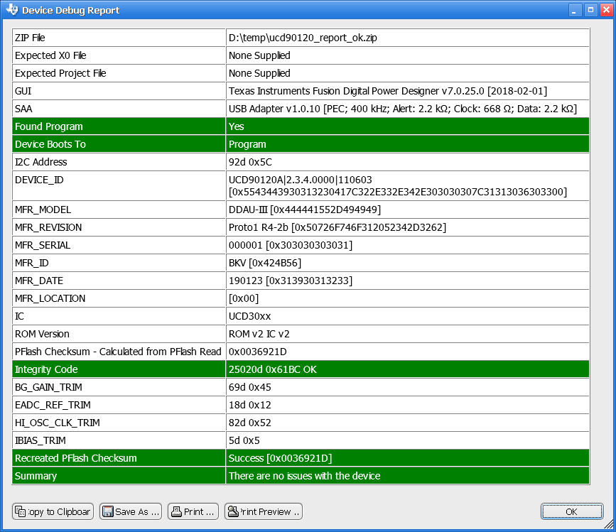
This time I have received 5 of the failed UcD90120As and have tested them in the UCD9064SEQ EVM.
There are a couple of interesting observations: (All 5 behave the same)
The I2C address is detected incorrectly:
I have set J13 to the two 84.5K resistors (shouldn't these be 90.9k?).
- With a OK UcD90120A this gives the I2C address 0x68 as expected.
- With a bad UcD90120A this gives the I2C address 0x5C which corresponds to one bin below for both PMBUS_ADDR pins.
When measuring the voltage on the PMBUS_ADDR pins during initialization, the voltage on a OK device is 0.86V and on a bad only 0.73V.
This indicates that the 10µA (+-1µA) bias current source is at 8.6µA for a bad device which is out of spec.
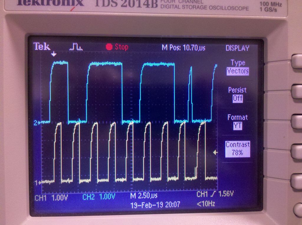
The EVM can communicate with the bad devices, but the I2C communication looks a bit different than for a good device:
On the bad devices, there is a short pulse on SDA just before the ACK and there can sometimes be seen a spike on SCK 0.5µs after the pulse on SDA:
(This spike messes with the I2C controller on our board which detects clock stretching. On the EVM, the T(SCK,low) is a bit longer (1.5µs vs. 1.25µs) and the 150ns low just after the spike barely hits the clock pulse)
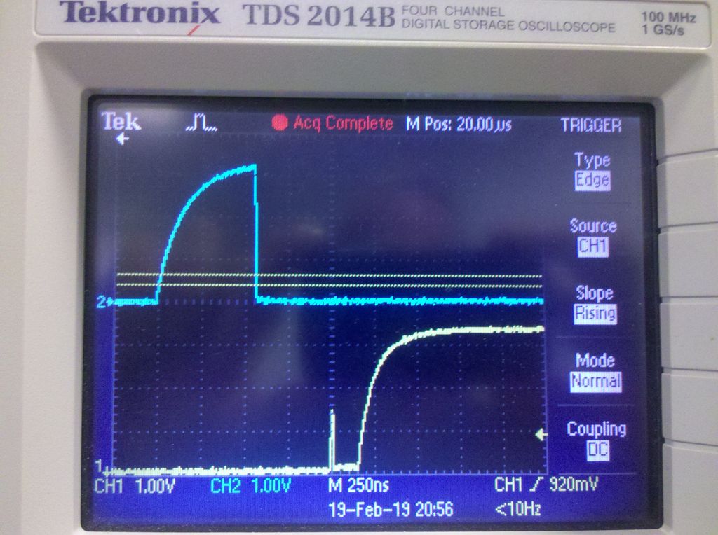
Zoomed in:
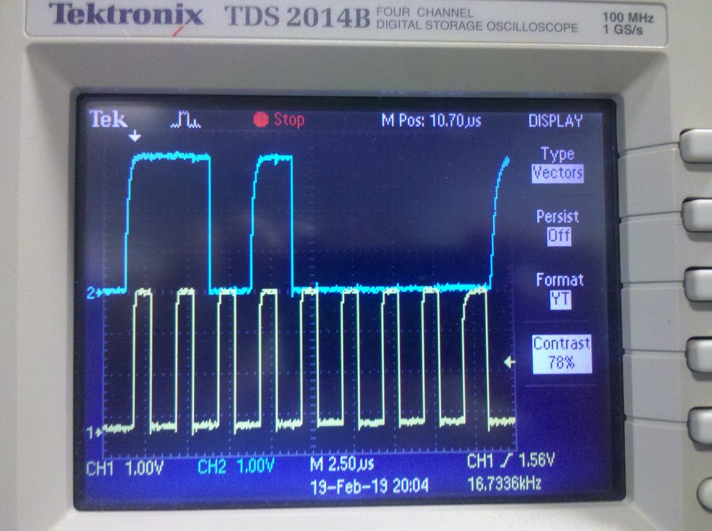
And a good device for reference:
These observations could indicate that some calibration (PMBUS_ADDR bias current and I2C timing) of the UcD90120A could be corrupted when programming the configuration via JTAG.
What could cause this and what can I do to avoid it?
I am generating the SVF for JTAG programming with Fusion Digital Power Designer and programming the devices with a Segger j-link Base using openocd under Windows.
Regards,
Søren M.