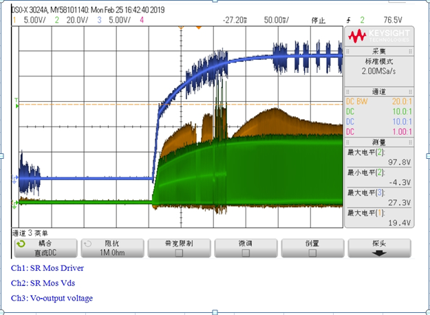
This thread has been locked.

If you have a related question, please click the "Ask a related question" button in the top right corner. The newly created question will be automatically linked to this question.

UCC24624: UCC24624 stress

Part Number: UCC24624

Hi Sir

we find the the stress during the startup of SR mos was too large during dubug UCC24624, do you have any solutions to solve this problem? The waveform is as follows

  • Hi, Darren,
    Can you explain to me how these waveforms are measured?
    The UCC24624 has internal LDO so that its gate driver voltage can only be up to REG pin voltage, which is 11V. In your waveforms, the gate voltage is above 15V. Can you help to figure out if this is correct?
    The second picture, you can see the SR FET voltage stays low after the gate voltage becomes 0 for about 100ns. Then its drain voltage shoots up way high. I am not sure what the circuit is doing to cause that. If the SR controller turns off too late and cause the negative current, you should see the drain voltage rise up right after the gate voltage becomes zero. Is it possible to measure the secondary side current and understand the circuit behavior?
    If only the start up give you the trouble, you can always delay the turn on by controlling the VDD voltage. Only provide the UCC24624 bias after the output voltage is close to the regulation level.
    Let's look into more details and figure out what is the best way to resolve this issue.
    Thanks.
    Bing