This thread has been locked.

If you have a related question, please click the "Ask a related question" button in the top right corner. The newly created question will be automatically linked to this question.

TPS63001: why does the converter TPS63001 always break by switching off the load and by charging the Lithium ion cell ??

Part Number: TPS63001
Dear People, good morning,
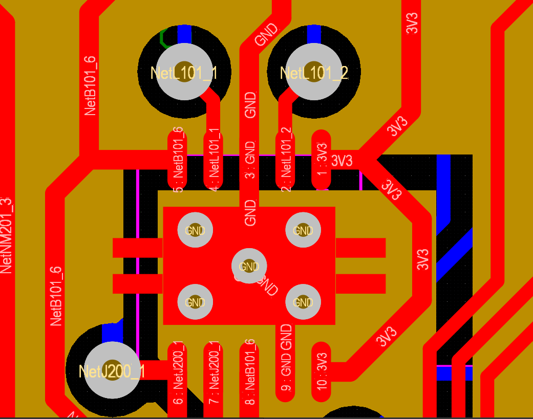
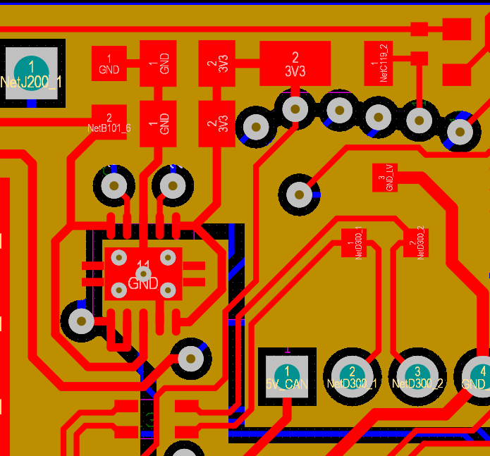
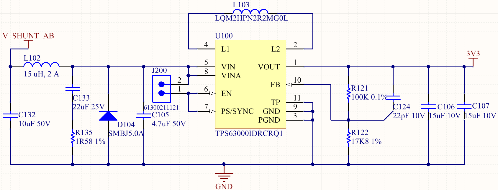
i developed a circuit from the boost buck converter TPS63001 with Vout = 3,3 V on a PCB according to the datasheet of TI. The component is supplied by a Lithium-ion cell (18650 mit 1,5 Ah). This means that the Inputs Vin, VinA , EN an PS/SYNC of the converter are directly connected to the positive pole of the Lithium cell. The converter has a Input capacitor of 10 uF X5R with 10 V as nominal voltage.
A load is connected to the Lithium ion cell via the circuit board. The load can be switched on or off via a NMOSFET. So far I have used ohmic resistor, elctronic load and incandescent lamp.
The Problem is that the converter always breaks when the load is switched off, although it has an Input voltage of 1,8 to 5,5 V according the datasheet and the cell is only operated with a rated voltage of 3,7 V.
I also tried to Charge the cell with the converter connected to the positive pole. However, the converter broke again, although the cell only hat a nominal voltage of 2,5 V and the charging cutt-off voltage was set to 3,,9 V. The converter was not working properly.
Why does the converter always break although the Input ranges according to TI are not exceeded?
I look forward to your help
Thank you
  • Hello Tchapi,

    thanks for your post.
    Could you please further explain what happens when the device "breaks"?
    Does this happen if you connect PS/Sync pin to ground?

    It could be useful to check your schematic and layout. You could share it here or via lbs_request@list.ti.com.

    regards,
    Julian
  • The PS/Sync Pin is always connect to Vin (positive pol of the Lithium ion cell). The Jumper is only use to Switch on the converter

    Thank you

  • Hello Tchapi,
    thanks for the schematics/layout. I see that there is a 100Ohm between VIN and VINA missing as well as a 100nF cap from VINA to GND.
    The power traces does not seem to thick. What is the maximum current that you support?
    Could you please describe what happens when the device breaks? (is this a failure that you have to restart the part?)
    Could you measure VIN, VOUT at the device with an oscilloscope when you disconnect the load?

    regards,
    Julian
  • Hello Julian,

    thank you very much for your Information.

    First. I didn't see any inforamtion about the 100 Ohm resistor and the 100 nF capacitor in the datasheet. The values were only set on the reference circuit without description. I did the simulation without the values and the results were successful.

    can you please explain me exactly what are the functions of those both components on the converter (100 Ohm and 100 nF)?

    current flow: the maximum load current is 300 to 500 mA.

    break. by switching off the load the converter break and the Output voltage is only 0,7 to 1,2 V. I didn't restart the part. I only switch off the load and the converter is connected to the Lithium ion cell. My guess is that a transciente peak voltage because of the inductance of the cell damages the converter. But actualy that should not happen because the load is only 300 to 500 mA.

    Vin: With the oscilloscope i measure a voltage of 7,9 V at the VIN Pin by swithing off the load.

    next design: Actually the plan was to use the converter with an 25 Ah Lithium cell and 360 A load current for 5s. With this confuguration the transciente voltage at the Simulation is 50 V for 8 us by the 360 A Switch off current. How can I protect the input of this converter against any transciente voltage???

    thant you for your answer.

  • Hello Tchapi,

    7.9V on VIN will damage the device as it is above the absolute maximum rating.

    For the next design, the load current is 360mA, correct?

    Your question: How can I protect the input of this converter against any transciente voltage???
    This depends on the root cause of the overshoot and the time it occurs.
    If it is ringing of the impedance from your source to the board (cable and connector impedance from battery to VIN pins), input impedance reduction will help significantly.
    It will help to reduce the length of the connection (cable or board layout). Make the connection wider, e.g. when I have a look at your design above, you are using only a small wire for connecting VIN and the input capacitor is far away from the IC, please review the EVM layout for low input impedance connection.
    In addition increasing the input capacitance will help a lot. Have a look at the EVM, we added a tantalum cap at the input because we expect people to use these boards with long cables (>20cm).

    If the root cause for the high voltage is different, like a sudden increase in the battery voltage when the load is removed (to be honest, I do not expect this, but as I do not know a lot about your system, battery, ..., I have to consider all possibilities), or any other root cause, you need to dig more into details of this issue. For this a good idea would be to order an EVM and check how high the voltage is going when a good board layout is used.
     

  • Hallo Brigitte and Julian,

    actually we didn't have any cable in our design. The converter is directly connected to the Input of the Lithium Ion cell through the PCB. The PCB is directly mechanic placed on the cell, so that a electrical Connection is etablished between the PCB and the pols of the cell.

    First Question: What are the fonctions of the 100 Ohm resistor and 100 nF capacitor at the VINA please? that was not possible for me to read any Information about that in the datasheet.

    Second Question: To reduce the transciente voltage at the Input of the converter I used a LC-Filter and a TVS Diode as you can see on my design. Do you think that the LC-Filter can be a Problem for the good fonctionality of the converter?

    Third Question: I read in some papers that it is a bad idea to use a tantalium capacitor in Connection with a Lithium cell because they are very sensitive to voltage fluctuations, which can cause short circuits in the capacitor. Do you agree this?

    Design:


  • Hello Tchapi,

    100 Ohm + 100 nF on VINA: This is a noise filter to reduce the coupling of the switching noise into VINA. Especially with a layout that is not optimized this optimizes IC function, but for sure this is not the reason that the IC gets damaged.

    LC filter on VIN: I wonder if this filter even increases the issue you have when turning off the load. The energy stored in the inductor when there is load needs to discharge to the input capacitors and therefore I expect that you might even increase the input voltage when the load is turned off. I think you should remove the inductor and just increase the input capacitor to have less overshoot when the load is turned off. 
     
    Tantal caps with Li cells: You mentioned that you measured 7.9V on the VIN pin. Did you measure directly from negative to positive pole of the battery as well? If yes, which voltage did you observe there? I never heard that the voltage on a LiIon cell is increasing to such a high voltage, so I expect that the high voltage on VIN is not caused by the LiIon cell, but by the impedance in your supply and ground paths.
    In general tantalum caps will get destroyed by overvoltage, so if due to any case overvoltage can occur in the system, it is important that the voltage rating of tantalum caps is above the maximum overvoltage.

    I think that the overvoltage is not caused by the battery, but by the overshoot caused on the output when the load is disconnected. In your design (PS/SYNC = high), the converter is allowed to return current to VIN when the output voltage gets too high. As you have 30uF on the output and only 4.7uF on the input, it is possible that this causes overvoltage on VIN. Please add capacitance on the input side and the voltage overshoot should be reduced.

  • Hello Tchapi,

    Please compare your layout with the layout of the EVM and try to adopt the EVM layout to the new board.