This thread has been locked.

If you have a related question, please click the "Ask a related question" button in the top right corner. The newly created question will be automatically linked to this question.

UCC21520: Question with the application

Part Number: UCC21520

Hello everyone,

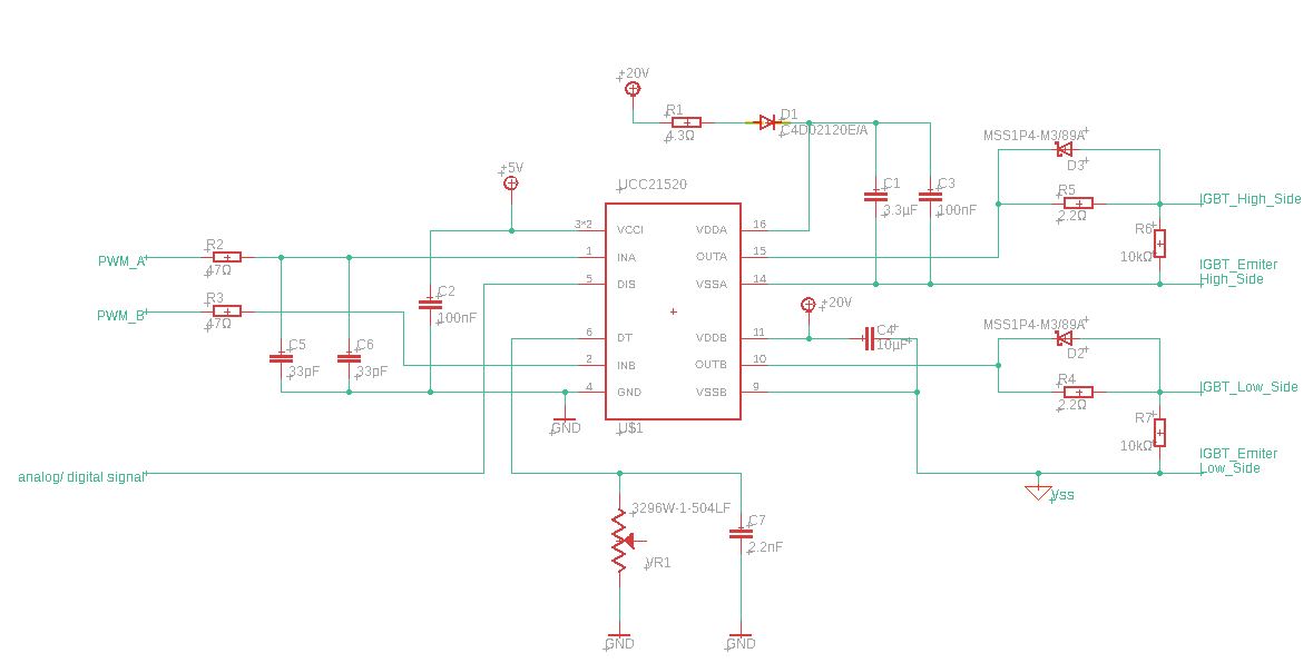
I'm trying to build a three phase inverter with the UCC21520. My design is based on the appliction which is described in the datasheet. In the design I've calculated almost all the passive components except for the resistor between the pins 14 and 15 and the pins 9 and 10. How do I calculate the dimensions for this resistor? In the datasheet it is not clarified how I should calculate it.

Thanks in advance!

  • Hi Gauthier,

    I'm an applications engineer in the high power drivers group and can help you with your question.

    I'm going to assume you're referencing Figure 38: Typical Application Schematic in the UCC21520 datasheet. That would mean you're looking at Ron, Roff, and Rgs. Section 9.2.2.3 covers how to size the actual resistance values for Ron and Roff. Rgs should be sized ~10kOhms and is there to locally pull down the gate when it is not being actively switched by the driver. This pull-down can be a smaller package size since it does not conduct much current or dissipate much power.

    Actual package sizes for the Ron and Roff resistors will depend on the amount of power dissipation and allowable temperature rise for each package. The resistors should be capable of handling high peak currents for the entire switching period as well. Power dissipation will depend on your selected FET's gate charge and can be calculated using Pgsw equation in section 9.2.2.4. RMS current can then be inferred from this Pgsw equation, and Ploss in Ron and Roff can be attained. Peak current will depend on the selected value of resistance as calculated in section 9.2.2.3.

    Depending on FET Qg and switching frequency, I've personally seen anything from 0402, to 0603, to 0805 resistors used in this gate drive loop.

    I hope this gave you a good place to start. Please feel free to share your schematic and calculations if you would like to ask more questions on the subject.

    If this helped answer your question, could you please press the green button?

    Thanks and best regards,
    John
  • Hello John

    Thank you for the help! I did some calculations and I added the circuit in this reply. The IGBT's I'm using are the BSM 150 GB 120 DN2 (datasheet: https://www.galco.com/techdoc/eupc/bsm150gb120dn2_dat.pdf)

    The switching frequency will be 16kHz, Vcc=5V, Vdd=20V and the HV DC-Link will be 600V. I think everything should work perfect, but it would always be nice if you could confirm that everything will work fine. Especially because it's my first time building a circuit and making my first PCB. Thanks in advance. If you need extra information I can always add it in this thread.

  • Hi Gauthier,
    Thanks for providing your schematic! That helps immensely.

    Some initial things on the primary side: I think C6 should be connected to PWM_B input instead of in parallel with C5. We recommend adding a 1nF capacitor close to the DIS pin (pin5) just to make sure noise on the high impedance net doesn't turn the device off. Make sure DT decoupling cap (C7) is located as close to the pin as practical.

    On the secondary side: It looks like the IGBTs you've selected can operate up to 20V Gate to Source, which means you will be operating right at the recommended max. This will probably be violated during switching transients which wouldn't be good. You can either lower this 20V supply, or you can go split supply and drive the IGBTs at something more like +15/-5, which is something we commonly see in our other customer's IGBT drive circuits. There are a couple different circuits to achieve this off a single rail 20V supply - Figure 39 in the datasheet gives a good initial design.

    Last thing: Is 16kHz a hard requirement? This will probably emit an audible high pitch noise. Going to 20 kHz would bring that sound out of the hearing range of most humans and is what we see in many of our customer designs. This also could help shrink inductor and capacitor sizes down the line.

    This is a very good initial schematic. Feel free to ask more questions!
    If this helped answer your question, could you please press the green button?

    Thanks and best regards,
    John
  • Hello John,

    Thank you for all the feedback you are providing! It is really appreciated!

    I considered some things you said in your previous reply. The capacitor C6 indeed was supposed to be connected to PWM_B I made this mistake while drawing the scheme probably. I have also added the 1nF capacitor at the DIS pin as you recommended.

    The voltage of 20V is indeed not perfect for the IGBT's so as you said I will drop the voltage to 15V instead. Do I have to change some components for this operating voltage? I think the boot capacitor should be smaller, but I'm not sure. I calculated the dimensions and the minimal capacitance should be 1.6µF. Can I still use the 3.3µF from my previous design or would it be better to take a capacitor with a smaller dimension?

    The operating frequency will probably stay at 16kHz, but can I work with the current design at 20kHz if I want? The inverter is for experimental purpose for my thesis so it would be nice to use the inverter on different switching frequencies. I added the modified scheme below in case you had extra remarks on it:

    Thanks in advance and thank you for all the help!

    Kind regards

    Gauthier

  • Hi Gauthier,

    Happy to help.

    The schematic looks pretty good now. If you wanted to run +15V/-5V on the output, you could keep the 20V input and generate the split supplies from this bias. Other than a split supply circuit, you shouldn't have to change anything to run at +15V only. Using 3.3uF should work well, it's just important to have the pads there if you need to modify it during your testing.

    It might be prudent to add a placeholder 0 ohm turn-off resistor in series with D2 and D3 so you can play with the output circuit's drive strength if needed. I've also seen the drive circuit reversed for IGBTs so there is a turn-on diode circuit instead of a turn-off diode circuit. 16 kHz should work, so no worries on that operating point.

    If this helped answer you question, could you please press the green button?

    Feel free to respond back with any other questions.

    Thanks and best regards,

    John

  • Hello John,

    Thank you I'll add the 0 ohm turn-off resistors as you suggested and I'll give the green light to build the circuit. Although I still have a small question left. The ground Vss is this a special ground or is this also considered a simple ground like the other cases? Furthermore I will not have any questions anymore.

    At last, I want to thank you for all the help you provided me on creating this circuit!

    Thanks and best regards,

    Gauthier

  • Hi Gauthier,

    That's awesome! Just remember to keep the high current loops small in order to reduce parasitic inductance when doing the layout.

    So, since this is an isolated part, the 'GND' and 'VSS' nets are all galvanically isolated from each other using TI's cap-iso technology. This means that the primary and secondary sides of the isolator can operate at different reference potentials. It also means that 'VSSA' and 'VSSB' nets are functionally isolated from each other and can operate at different potentials. That is what allows you to use this part as a high voltage half bridge driver, with VSSA referenced to the switch node/upper IGBT emitter, and VSSB referenced to the lower IGBT emitter.

    Going forward, it would be beneficial to think about things in terms of 'reference potentials' instead of 'ground'. Depending on how the VCCI (5V) and VDDB (20V)  rails are generated, 'GND' and 'VSSB' can remain isolated from each other. If needed, you can tie 'GND' and 'VSSB' nets together to attain the same reference potential, though you will lose the reinforced isolation from primary to secondary sides. In this case, more care would need to be taken to keep sensitive analog and low-voltage digital circuits out of the high di/dt switching currents.

    All of this depends on the isolation requirements of your power supply. Feel free to watch our TI Precision Labs videos on Isolated Gate Drivers which covers the main aspects to care about when designing your system.

    Thanks and best regards,

    John