This thread has been locked.

If you have a related question, please click the "Ask a related question" button in the top right corner. The newly created question will be automatically linked to this question.

ISO5452: Added RC Circuit for STO - Increased Switching Losses

Part Number: ISO5452
Other Parts Discussed in Thread: ISO5852S

Hello, 

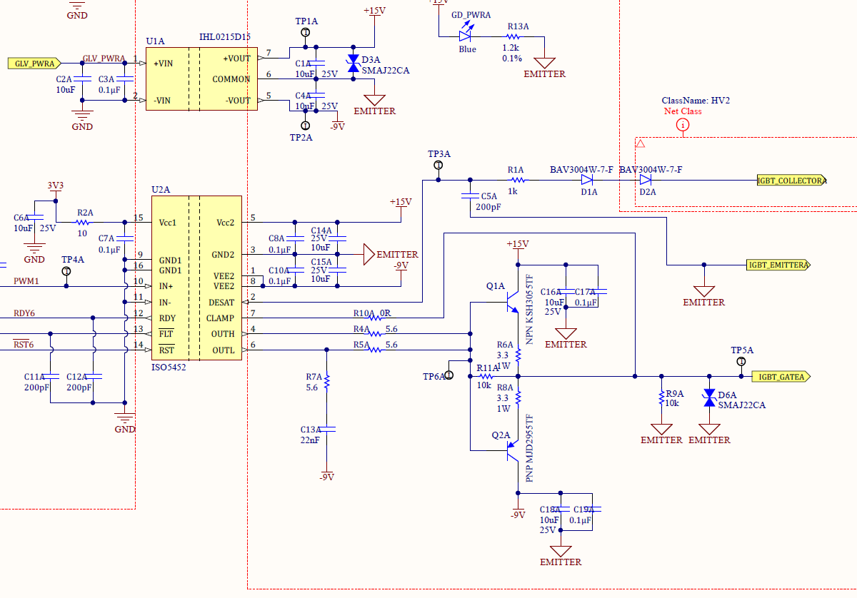
I'm working on an IGBT gate driver design using the ISO5452 + totem-pole current amplifier.  To implement desaturation detection, we added an RC circuit to OUTL because off the totem pole amplifier as recommended here

The problem is that with the added capacitance to the gate, I expect turn-off time and, in turn, switching loss to increase quite a bit. Is there any clever ways to get around this? 

Thanks!

  • Hi Jason,

    thanks for asking on e2e,
    Can you tell me which RC on OUTL gate your referring to?
    R7/C13 snubber or R11/and another capacitance?
    desaturation detection does not require anything to be put on OUTL since there is a dedicated DESAT pin to allow a blanking time.
    The DESAT detection can speed up by putting a cap parallel to each resistor as seen on slide 22.
    let me also reach out to the ISO driver team to help you out with this question.

    thanks,
  • Hi Jason,

    I am an applications engineer in the Isolated Gate Drivers group.

    As Jeff mentioned, slide 22 of the attached power point discusses how capacitors can be added in parallel with the resistors of the DESAT circuit to speed up the DESAT response time, but result in higher switching losses. With regards to the DESAT circuit, there is not a recommendation to add R and C to the gate connection.

    Can you specify which R and C you are asking about in your schematic? What slide in the power point are you referring to?

    Thanks and Regards,

    Audrey
  • Hi Jason,

    I believe you referring to R7A (5.6 ohms) and C13A (22nF). Is that correct? This RC circuit, as you mentioned, is required to adjust the speed of the Soft-Turn-Off (STO) when a totem pole buffer is being used. You are correct that your switching speed in normal turn-off will be affected by this RC circuit. If the RC circuit is not used in this case, you will not be able to adjust the STO time. Luckily, you will still have the benefit of a high source current during your turn-on transient, and thus lower switching loss at turn-on due to the BJT buffer. However, at turn-off your maximum current sink is dependent on the value of R7A. My recommendation is to adjust the circuit to find a balance between your allowable turn-off switching loss and required STO timing.

    If you need additional support with your STO timing circuitry or have other questions, please let us know!

    Thank you,
    Audrey
  • Hiii Audrey,
    I am developing a SIC gate driver with ISO5852s. I am using external current buffers FZT851 & FZT951. The turn on & turn off resistors are 3.9ohm, 3.9ohm, turn voltage is +15V, turn off is -5V . The Ciss of the SIC mosfet is 16nF , short circuit withstand time is <= 2us. Please help me to decide the R & C values of STO to get a soft turn off time of 1.5us.
  • Hi Naga,

    The ISO5452S has a low-level output current of 130-mA after a short-circuit condition. The capacitor is based on this current, thus you can calculate the value using the equation C=(t*I)/(VCC2-VEE2), where t is 1.5us, I is 130-mA and VCC2-VEE2 is 20V. Using these parameters, you'd find a value of C=9.75-nF. The value of the series resistor is based on the current level during normal turn-off operation, which is 5-A. Thus, R should be greater than (VCC2-VEE2)/I, so R must be at least (20V)/(5A)=4-ohms.

    Regards,
    Audrey
  • Hi Naga,

    Please refer to this attached app note where we achieve 3us of STO time on a 15nF load. This design uses R10=12-Ohms and C39=15nF. You may start with a set capacitor value (1-10nF) then tuning your resistance accordingly to achieve your 1.5us desired STO.

    Section 2.1.7 and 4.3 below discuss this in further detail.

    www.ti.com/.../tiduc70a.pdf

    Please let us know if you have further questions.

    Regards,

    -Mamadou
  • Why it is needed to connect the two bases ? why can’t we operate separately. 

  • Hi Naga,

    If the IGBT module is directly connected to the gate driver IC, the gate charge of the IGBT is slowly discharged through the internal current sink of the Isolator during turnoff.

    The BJT buffers (between the driver and IGBT) help increase the IGBT gate drive current therefore in the event of a short circuit, you need to provide the soft turnoff of the device and that must be done directly at the driver's output which are connected to the base of the transistor pairs.

    Please let us know if you have further questions.

    Regards,

    -Mamadou
  • I think you have not understood my question. In the image that I have attached above, mentioned to connect the bases of the pnp, npn. Here my question is it mandatory to connect the bases?

    Can we operate the circuit without connecting the bases?

  • Hi Naga,

    My apologies, You're correct I misunderstood your question.

    To answer your question, yes, you must connect both bases of the pnp-npn pairs to configure as non-inverter buffer for the BJT buffer to achieve the desired increase drive current. Both bases connected would then be connected to the split output OUTL and OUTH through resistors.

    We do not recommend connecting one base to OUTL and the other base to OUTH or using inverting current buffers as desaturation fault protection will not be compatible with this configuration.

    I hope this answered your question. If it did, please press green button or let us know if you have further concerns.

    Regards,

    -Mamadou