This thread has been locked.

If you have a related question, please click the "Ask a related question" button in the top right corner. The newly created question will be automatically linked to this question.

TPS40210: Schematics and Layout review for the PoE Boost converter

Part Number: TPS40210
Other Parts Discussed in Thread: TLV431, PMP, LMV431

Dear Team,

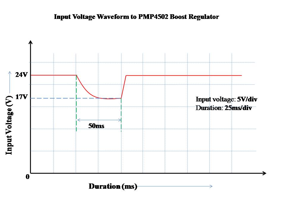
We are using TPS40210DGQ boost regulator for converting 24V to 48V output for PoE application.

We have referred the below link for the boost regulator design (PMP4502 using the above mentioned regulator part),

Please find the Schematics and Board file enclosed within for the review.

Request you to please review the same and let us know for any concerns.

Also please let us know what will be the output of the above circuitry with input 19V. We need to support input voltage for 24V +/- 20%.

Kindly let us know on above inputs at the earliest.

Regards,

Nibinhttps://e2e.ti.com/cfs-file/__key/communityserver-discussions-components-files/196/TI.7z

  • Hi Nibin,

    Just let you know that we received your request and I am able to open your compressed file. We will review this and get back to you next week.

    Thank you for considering the TPS40210 in your design.

    Best Regards,
    Youhao Xi, Applications Engineering
  • Dear Youhao Xi,

    Thank you for the reply.

    We are in final Gerber release stage, so we need the inputs at the earliest preferably by today.

    Also please let us know what will be the output voltage of the boost regulator circuit (with TPS402100) when the input is 19V.

    We need to know on the above inputs at the earliest.

    Awaiting your response.

    Thanks and Regards,

    Nibin

  • Dear Youhao Xi,


    Awaiting your response.


    Thanks and Regards,
    Nibin
  • Hi Nibin,

    I just replied but somehow my reply was lost. Let me re-do it below.

    First the schematic looks okay, although I would like to ground the SD pin. Leaving it open is okay per datasheet. No big deal.

    Regarding your layout, it basically look good. My comments below:

    (1) use the thick copper strip on the surface to directly connect the current sense resistor ground pad to the output capacitor ground pad (C743?). Always try to avoid using via holes to conduct power current.

    (2) do not waste PCB area. Alway try to fill up PCB void with ground copper polygons. This helps improve the board structure strength, thermal performance, and noise shielding. I see a lot of void areas.

    (3) input and output capacitor ground pads should be connected on the surface layer with wide copper polygons. If you want to conduct current to the inner layers, use multiple vias holes for each capacitor. Currently I only see one via hole beside each capacitor ground pad.

    (4) Your gate drive trace overshadows your current sense trace and this may couple the gate drive noise to the current sense signal. Please separate them away to avoid noise coupling.

    (5) Current sense signal should be picked up directly at the sense resistor, although the MOSFET source and the resistor are on the same polygon. Please re-route the sense trace to the resistor pad.

    (6) In a boost circuit, the critical ac current loop include the following component: the MOSFET, current sense resistor, the output capacitor and the diode. These part should be placed closely, and the pcb trace should be routed such that current flows in direct and straightforward direction without enclosing large spatial area. I think you can move the inductor and diode closer to the MOFET to minimize the ac current loop.

    (7) You may consider to add thermal vias under both the IC and the MOSFET drain pad. By doing so, you should repeat the underpad polygon on all PCB layers, and leave the other side exposed.

    Wish these help.

    Best Regards,
    Youhao
  • Dear Youhao,

    Thank you for the feedback.

    We will implement all the layout suggestions.

    Also please let us know what will be the output voltage of the boost regulator when the input is 19V to the boost regulator.

    Thanks and Regards,

    Nibin

  • Hi Nibin,

    at 19V the peak current limit might be triggered. The solution is to reduce the current sense resistor values. I think your circuit should support your entire operating range, just a matter of fine tuning of a few part values.

    Thanks,
    Youhao
  • Dear Youhao,

    Thank you for the response.

    Our designs input operating voltage is 24V +/-20% ( 19V to 29V). This input is same as the input to the above mentioned boost circuitry.

    We under stand that with the input 19V to 29V the boost circuitry will give 48V output if fine tuning is done.

    Please let us know how to tune the boost circuitry permanently so that any input voltage between 19V to 29V will provide 48V output in all cases.

    Regards,

    Nibin    

  • I did a quick calculation and the peak current at Vin=19V may trigger the OCP. Slightly reduce the current sense resistor should be the only thing that you need to do. If you make significant value change in the CS, you may need to adjust the loop compensation. But save this effort until necessary: test first and see if your circuit is able to supply full power at 19V.

    Thanks
    Youhao

  • Dear Youhao,

    Thank you so much for the support.

    We need to support the below input waveform for PMP4502 circuitry.


    We need to know exact modification in the current circuitry of PMP4502 (24V to 48V boost converter) to meet the above input voltage requirement (30% voltage dip for 50ms).

    The output voltage requirement in above case is 48V @ 350mA.

    Please let us know whether the above input requirement can be supported in PMP4502 design with exact change details at the earliest.

    Thanks and Regards,

    Nibin

  • Hi Nibin,

    This 17V is less than the 19V that you mentioned earlier. What is real, the 17V or 19V?

    The 50ms is almost a dc condition for the circuit switched at a few hundred KHz. If this is true, your circuit must guarantee operation with 17V input.

    The ref design supports 1A@48V load with 24Vin. When your load drops to 0.35A, the original design should support your full load at 17Vin. My previous concern of possible tripping the peak current limit was under the assumption of 1A load.

    Thanks,
    Youhao
  • Dear Youhao,

    Thank you so much for the quick response.

    Our customer is requesting for the design support of 30% input voltage drop. So considering 24V as normal voltage, the 30% dip will be around 17V.


    Now we understood that the output of the boost regulator (PMP4502) will give proper output 48V for the 30% input voltage drop occurs for 50ms.

    If the input voltage drop to PMP4502 circuitry is 60% drop (9.6V), whether the output 48V will be present? Customer is expecting the OFF of POE circuitry at this condition.

    Is it correct?

    Awaiting your valuable response.

    Thanks and Regards,

    Nibin

    Regards,

    Nibin 

  • Hi Nibin,

    At 9.6V I am afraid the circuit may be still be operating but it just be unable to support the full power because of the peak current limit. There is not UVLO control in the PMP design. If you want to turn of the device, you should consider to use a LMV431 or TLV431 to monitor the input voltage by setting a threshold voltage, and use the LMV431/TLV431's cathod to control the SD pin. There should be a pull up from the input line to the cathode through a large resistor (>20k). Thus, when Vin is below the threshold, the LMV431 cathod would be open, and the pull up will set SD pin high potential, and the TPS40210 will stop switch.

    Thanks,
    Youhao