This thread has been locked.

If you have a related question, please click the "Ask a related question" button in the top right corner. The newly created question will be automatically linked to this question.

TPS54202H: IC damaged

Part Number: TPS54202H
Other Parts Discussed in Thread: TPS54202

Hi All,
I use TPS54202H as a 12V to 3.3V converter with a small load of 100mA and a peak of about 500mA (MCU, WiFi module, LoRa module). On the same bus of 12V another TPS54202H is used to supply 5V to canbus peripherals. Similar circuit, same PCB layout. Sometimes, when a 300W DC motor powered from the common 12V battery voltage is started or stopped(PWM controlled), the 3.3V converter is destroyed. The other converter of 5V is unaffected. This happened three times in the last two months, quite rare and difficult for troubleshooting, but enough to ruin my project. After examining the corrupted IC I found that there is a shorting at the low side output FET, with a few ohms resistance between SW and GND. Do you have any idea why this is happening? Would it help if I put a TVS diode at SW, or VIN or even both pins with GND? Any suggestion is welcome.
Thanks in advance,
Panos

  • hi,

    I am looking into this question and will give you feedback on Monday.

  • Hi,

    Please test the waveform (VIN,SW,VOUT,IL) to check if the spike of SW is too large during the start or stop of DC motor.

    Could you please share the schematic and layout? Let's review it.

    Shawn

  • Hi Jason, Shawn thank you for your reply.
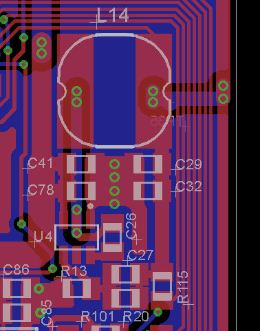
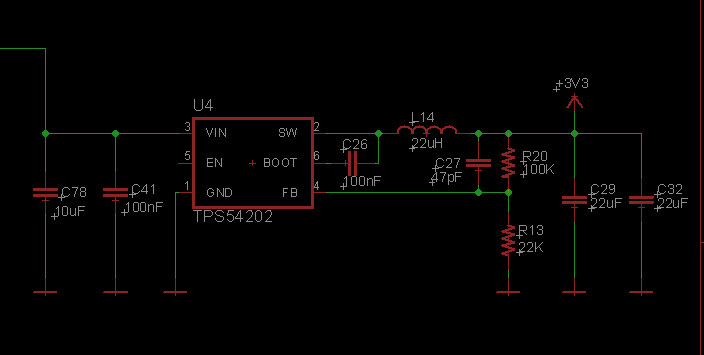
    Unfortunately I have no PCB in my hands and so I can not make the measurements you asked for. The schematic and PCB layout is as you see below:

    It is designed for TPC54202, but on the first batch of 16 PCBs, it was ordered and placed by mistake the device TPS54202H. I had to put a 510K pullup resistor between VIN and EN to make the circuit work. I soldered the resistor roughly 'on the air' over the IC, and mechanically fixed it with a drop of epoxy resin. In my opinion, the problem was due to some overvoltage caused by the back EMF of the motor, in conjunction with a ringing of SW output. The voltage at the SW terminal exceeded the absolute maximum of 30V and the FET was shorted.
    I am now in the process of redesigning the circuit with a view to assembling a new batch of 100 PCBs, and since the deadline has expired, I would urgently add a protection to the IC. Of course the correct type of TPS54202 will now be ordered, and pin EN will be left unconnected, as in the schematic.
    What would you suggest in this case as a preventive action to protect the IC?
    Thank you for your effort,
    Panos.

  • Hi,

    The layout is not good, the trace near SW pin is too thin, and only one via is used.
    You can add a boot resistor or a snuber circuit between SW and GND to reduce the spike voltage of SW.

    Shawn
  • Hi Shawn, sorry for the delay.
    Τhank you for your suggestions. Since I have not any time for trials, I decided to add a SMAJ15 TVS near VIN, a boot resistor to reduce ringing, and to improove PCB layout. I hope all theese whould help and I'll not have any damages in the new batch.
    Thanks again,
    Panos