This thread has been locked.
If you have a related question, please click the "Ask a related question" button in the top right corner. The newly created question will be automatically linked to this question.
Hello Community,
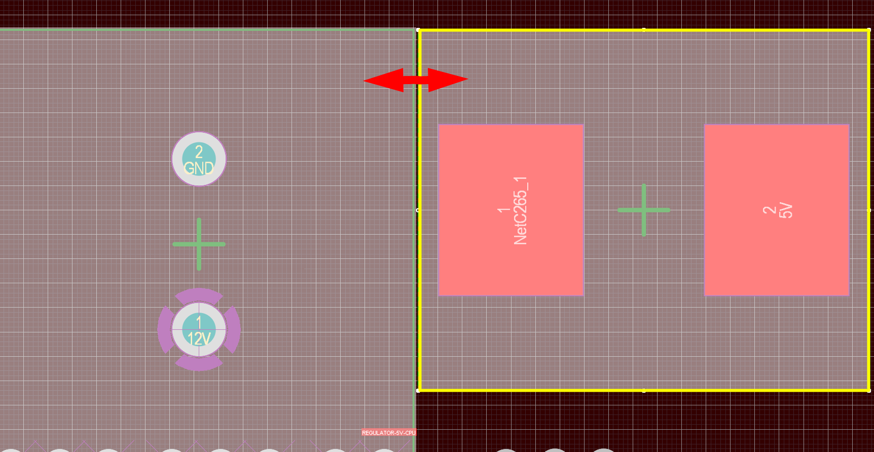
1. Tell me, is it necessary to isolate (cut copper) the area (placement area) located directly under the inductance from any passing signals, for example, from passing GND? (yellow border)
2. Is it necessary to indent elements of topology (capacitors, etc.) from the inductor if it is fully shielded? If so, what should be its value? (red arrow)
Description:
Left - Capacitor (VIN), Right - Inductor (VOUT)
Hello Anthony,
1. Please tell me how to choose the correct value of inductance to voltage, which is not in the table (3.8V). Webbench selects 2.2uH. But I would like to understand by what principle this is happening.
2. What principle is chosen for irms / isat inductors, what should be the supply of these values compared with irms / ipeak obtained in the calculations?
3. Still could throw off the links describing di/dt, dv/dt?
Thank you for the information you provided! I studied everything in detail and I had the last questions.
1. In the TPS563200 and TPS565208 Specifications, I noticed a different PCB layout, namely the top GND layer underneath the microcontroller. Do you think this is the right approach? (on the picture - red border) Can I use this approach in the case of the TPS563200? Will this technique increase EMI resistance?
2. Why are none of the specifications near the GND pin having transfer holes when each capacitor has 2 pieces on each? Are vias needed to reduce the current trace near the output of the GND converter (PIN # 1)?
3. Can I use ECAS (Murata) series polymer capacitors as output capacitors?
4. WebBench contains errors regarding the number of required capacitors provided by the specification. Example: instead of 2 output capacitors, it puts 1 on their total capacity. Please correct this.