This thread has been locked.

If you have a related question, please click the "Ask a related question" button in the top right corner. The newly created question will be automatically linked to this question.

TPS82130: EN Pin Behavior in Inverting Configuration

Part Number: TPS82130
Other Parts Discussed in Thread: TIDA-01457

Hello

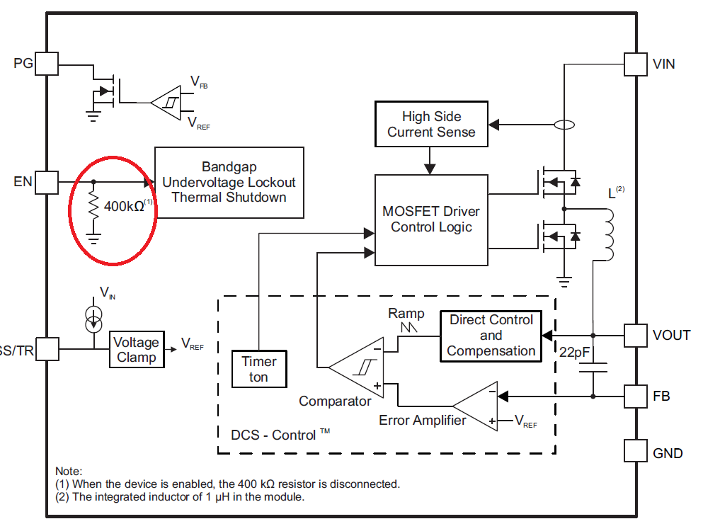
When I'm using TPS82130 in inverting configuration, as indicated by the application note TIDUD32.

As stated in the app note, when Q2 is OFF "the EN pin is initially at the levelof the output voltage(–5 V), whichis below the low-level threshold, and disables the device." (second paragraph, page#7, TIDUD32)

My question is when VOUT (negative voltage) isn't even available before the device is enabled, how is the EN kept below threshold? Essentially if there is no VOUT present, then EN is floating, isn't it, therefore can't be guaranteed to be below the threshold and therefore can enable the device before disbaling itself owing to EN being pulled down to VOUT in a vicious cycle of sorts?

Regards

Atin

  • Hi Atin,

    Thanks for taking the time to go through the application notes.
    As mentioned on page 5 and page 9 in the datasheet, an internal pull-down resistor of 400kΩ is connected to the EN pin when the EN pin is Low (i.e. when the device is disabled). The pulldown resistor is disconnected when the EN pin is High.

    Best regards,
    Omar
  • Hi Omar

    Thanks for your reply.

    Kindly refer to Chris Glaser's reply to another post e2e.ti.com/.../2710298 where he says, "If the pin is low, and then floated, it will be kept low by the 400k." which implies that to be held low, it has to be pulled low once. And later as well he says, "Yes, you need to drive the pin high and low. This is also written on page 3 of the D/S."

    Even if that's not true and the internal pull-down does pull EN down by default, in case of TPS82130 being used as inverter, to what voltage will it be pulled down to? Because GND is now connected to VOUT pins and output is connected to GND pins. 

    As you can see the pulldown is to GND but in case of inverterit will be replaced by a negative output voltage, since the deivce hasn't been enabled, this negative voltage won't be present. Therefore to what voltage level is the EN pin pulled down to when being used as an inverter?

    Regards

    Atin

  • Hi Atin,

    Thanks for your prompt and detailed answer.

    It is always advisable to drive your enable signals high and low to have precise control of your IC.

    In your application, the EN pin and Vout are connected together. However, when the system is starting up and no Vout is present yet, the EN pin is at the same level as Vout and they are both pulled to the system's ground.

    You can clearly see how both pins behave in figure 24 and 25 in the TI ref design TIDUD32.

    Best regards,

    Omar

  • Hi Atin,

    I have not heard back from you, so I hope that you issue is solved!
    I will close this thread for now; in case you have further questions, just reply below.

    Thanks and best regards,
    Omar
  • Hi Omar

    I was trying to understand the complete breadth of what you had mentioned. I still have few questions.

    As you said "how both pins behave in figure 24 and 25 in the TI ref design TIDUD32" - I assume that the probe that you're using has an impedance of 1M or 10M, and when you probe, you're connecting the probe's reference to the GND on the eval board which means when you probe the EN pin you're pulling down EN to GND through a very week pull down resistor. Therefore, in both cases when EN is floating and when its pulled down to GND, the moment you probe the EN pin it will show the same behavior as in the figures 24 and 25.

    Secondly you also said "when the system is starting up and no Vout is present yet, the EN pin is at the same level as Vout and they are both pulled to the system's ground." How is that happening? Can you share the output stage with EN pin configuration to show this? Because from my understanding the EN is referenced to GND pin voltage, whatever that may (or may not) be, which means that if GND pin is floating then EN is floating.

    Consider it like this, take a NAND Gate, connect 5V to its voltage pin, connect one of its inputs through a resistor to the GND pin but do not connect the GND pin anywhere. Now can you tell me what is the voltage on that pin? In my view, its indeterminate but I might be wrong.

    Regards

    Atin

  • Hi Atin,

    At any node in the circuit, there is a discharge path to the ground. In this situation, the discharge path is the feedback divider that will be responsible for discharging and pulling the EN to ground.
    Please read section 2.3.4 again and refer to the figures associated to it. It is explained there how the EN pin is pulled down showing that it is not floating. Furthermore, before the system is started up, the EN and Vout have a 0 voltage, which is ground level.

    Regards,
    Omar
  •  Hi Omar

    I went through the relevant section and I've attached my understanding of what you wanted to convey. Let me know if that is correct? If it is correct then it means that the pull-down on EN pin no longer 400K but 400K+ FB_Path resistance.

  • Hi Atin,

    Let me explain how the operation of the enable process in the design in TIDA-01457 works and I hope this would clear any doubt you have about this “multiple grounds” issue.

    So let’s first take TPS82130 alone in normal operation as a buck converter. It has an enable pin that is pulled down to ground to avoid any accident start up. To enable the device, a logic high signal ≥ 0.9V is needed. In case a logic low signal ≤0.3V is present at the EN pin, the 400kΩ internal resistor will keep the EN pin pulled low and thus disabling the device.

    Now let’s put the TPS82130 in the inverter design in the TIDA-01457. In this design, the “IC ground pin” is the Vout. As a result, the EN pin will be referenced to Vout (which is the IC ground pin) instead of ground (absolute ground). Due to this, the EN pin values for “high” and “low” signals are now different, because our reference now is Vout. Therefore, the high signal threshold is ≥ (0.9V + Vout) and the low signal threshold is ≤ (0.3V + Vout).  As a result, if the TPS82130 is operated in this inverting configuration, it will need a special circuit to control the enabling and disabling of the device. Therefore, the EN Pin Level Shifter is introduced. This circuit simplifies the process of controlling the EN pin. I do not think I can explain it better than the reference design, so please refer to page 7 in the reference design to understand its concept. Moreover, please pay attention to the 1MΩ resistor on the right hand-side of the EN Pin Level Shifter circuit that is pulling EN to the "IC ground".

    Finally, in the start-up of the whole system, there is not Vout present at the “IC ground pin” so the EN pin and the “IC ground pin” will have the same voltage level. Furthermore, we established that in this configuration, the enable high signal is (0.9V + Vout) which is not the case here and this is how the device is kept disabled until the signal SYS_EN in the Level Shifter Circuit starts enabling and disabling the operation.

    I hope this makes it clear.

    Best regards,

    Omar

  • Hi Atin,

    I am writing to follow-up on the status of your question.
    Did my last post answer your question?

    Best regards,
    Omar