This thread has been locked.

If you have a related question, please click the "Ask a related question" button in the top right corner. The newly created question will be automatically linked to this question.

BQ76930: BQ7693003 Different temperature readings on TS1 and TS2

Part Number: BQ76930
Other Parts Discussed in Thread: BQ76940,

Hello,

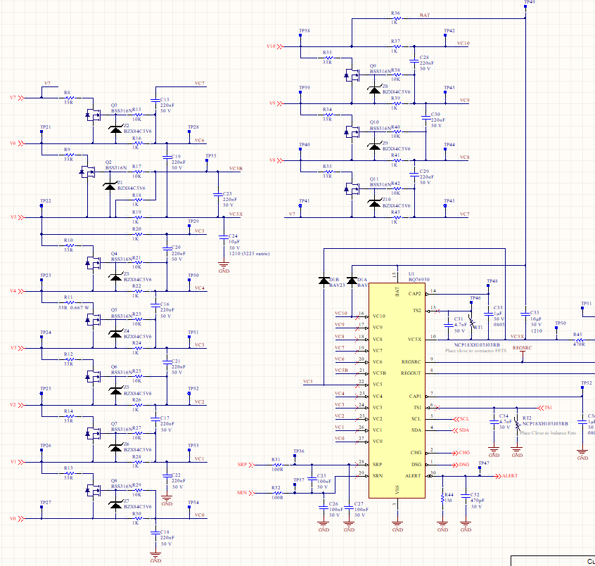
in my design for a 10S battery I have a 10K NTC each in between TS1 & VSS and TS2 & VC5X, both also decoupled with a 4.7nF capacitor.

At room temperature I notice a temperature reading difference of ~3C, but when I cool the NTC's with freezing spray I

see the temperature reading on TS2 drop accordingly but on TS1 it won't go below 14C. My boot circuitry is connected

via a diode and I checked the voltage on the anode side after boot, which is 0V. To be sure of no interference by the

boot circuitry I inserted a switch and disconnected it completely after boot. The reading on TS1 remained unreliable.

Hereafter I replaced the NTC's by fixed 47K resistors but to no avail: TS2 now gives -10C (after conversion) and TS1

14C!

If I measure with a scope (with the 47K's) I see on TS1 a periodic pulse of 50msec wide, 2Vtt every 2 secs, while I see

on TS2 the same signal, but with a Vtt of 2.75V.

The voltage on REGOUT = 3.3V and stable.

Any ideas?

  • Hi CP,
    As you know the thermistor resistance will vary with temperature. When hot the temperature goes down, when cold the temperature goes up. Since the high resistance (47k) you added did not let the TS1 voltage go as high as expected, something must be adding some resistance or load to the net. TS1 has a boot circuit which TS2 does not. Check the boot circuit carefully for leakage. Also check for contamination on the IC pin or trace. If several boards do the same thing it is more likely to be a circuit issue. If one board does it it could be contamination or damaged IC.
  • Hi WM5295,

    as already described I inserted a switch into the boot circuitry to have it removed completely after AFE boot. There for sure is thus NO leakage from that as neither there is contamination. We currently have 3 different designs around the bq7693003 and ALL 3 show the same behavior, on different boards and on different versions of the designs. We also have a design around the bq76940, but there the TS1 (with an identical boot circuitry attached) shows correct behavior. This morning I replaced the 47K resistors with 3K3 versions and then both TS1 and TS2 reported 57C. It thus seems that the internal LDO for the thermistor does not operate on the specified 3.3V. However if I measure the voltages on CAP1 and CAP2 they both are 3.29V on all situations.
  • Hi CP,
    That does not sound normal. The internal design of the bq76930 and bq76940 is supposed to be the same. If the behavior is different between the parts and the bad behavior is consistent across multiple boards it would seem to be either in the circuit or the condition the parts have been subjected to.
    There should be an internal 10k resistor switched to CAP1 during the temp sample, it forms a voltage divider with the external thermistor or resistor to give a voltage which the MCU must convert to a temperature. If you remove the resistor/thermistor you should be able to see it go to the CAP2 voltage, the scope probe will pull down some of course.
    Since you have seen a voltage difference and limit on TS1 of 14C it would seem there is some pull down or limit of the pin voltage. 14C would correspond to about 15k, and a 15k pull down with the 10k internal and 3.29 V measured voltage would give 1.97 or about the 2V measured. Something limiting the voltage would also be a possibility, 15k parallel with the 10k thermistor at 25C should be a lot more than 3 deg error.
    I would still recommend looking for some unexpected circuit feature on the bq76930 design. Sometimes connections can exist on designs which are not obvious and they can be propagated to new designs through re-use. You will know your system best.
    If you remove the IC or lift the pin you can check the net for load. With the pin lifted you can check the voltage.
    If you replace the IC with one which has not had previous test it should remove a history of stress on the IC. If you believe the IC is not meeting its specification check with your supplier on returning a few parts for analysis.
  • Hello WM5295,

    I did what you suggested: I lifted the pin and performed a measurement. Lifting the pin now required a switch in between the pin and the pad as otherwise the device would not boot ;-). 

    As a result things got a little bit more obscure for me: after opening the switch, the reading now reports -45C (so a very high resistance -> i.e. as could be expected) and the measurement on the pin showed a 50ms square pulse of 3.3Vtt!!. So the device seems capable of lifting the pin to 3.3V. But..........with a load of 47K (also quite high....) it won't go to the desired level as then it resulted in 14C instead of -10C (2Vtt instead of 2.75Vtt) while with a lesser load of 3K3 the reading was more or less correct (57C), which to my assumption required a higher current into the resistor. I measured the load on the pin and that was what it should be, i.e. I could not measure any other load than the attached NTC.

    It looks to me that for some reason the LDO is limited in its current capability. The voltage on VC5 is 18V and stable, which is for what I could find in the datasheet the supply for the LDO. What could be limiting thie current? Or is there another explanation for the behavior?

    Just to be complete I hereby include the relevant part of the circuitry around the AFE. The Boot Circuitry is attached to TS1 via a diode on another page, but was disconnected via a switch in all relevant measurements.

  • Hi CP,
    That is an odd behavior. I would describe it as a voltage related limit to the TS1 pin rather than current but obviously they are related. The current from the TS1 pin with the external 3.3k (10k internal + 3.3k external) should be higher than with the 47k external (10k internal + 47k external).
    The supply for the LDO is the VC5X pin. As the TS1 pin is loaded you may see VC5X move some during the time TS1 has the pulse. As the TS1 and TS2 drift with respect to each other in time you can normally see VC5X move slightly up and down. You might check all solder joints on VC5X, a floating pin might cause odd behavior, but would not be expected across multiple boards unless it is in the solder stencil and would likely show some issue in another measurement.
    If the limit is with the pin attached to the board there might be something unexpected on the board. If the pin won't reach the right voltage when lifted and loaded with a known resistance it seems the part pin must have been damaged somehow. This seems odd since you have working bq76940 designs which presumably would have been processed similarly.
  • Hello WM5295,

    well......odd is just an understatement until you find the cause....and then odd just becomes plain stupid.

    It had to be something related to the design, as 3 products based on the same design showed the behavior on all assemblies. So it could not be anything with contamination, broken parts, solder joints etc etc etc. And indeed you were in a way correct with your initial assumption that there could be some leakage in the boot circuit. Well...there was...but not directly in the boot circuit. The thing was that the TS1 pin was protected by a 3V3 Zener diode directly on the pin....and although the voltage on TS1 remains way below 3V3 all the time (even during boot), the Zener naturally still draws some current below its Zener voltage. Removing the zener (or better: reconnecting the zener to the anode side of the separating diode) did the trick.

    All in all thus a tempest in a teapot .

    Many thanks for your time and patience.