This thread has been locked.

If you have a related question, please click the "Ask a related question" button in the top right corner. The newly created question will be automatically linked to this question.

TPS25982: TPS259824ONRGE

Part Number: TPS25982

Hello,

I'm designing a card with TPS25982 OCP function, and some application have questions.

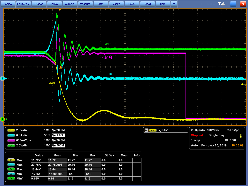
(1) The waveform is Vout short ground while power on, peak max VIN is 18V.
Would you can suggest a way to stabilize waveform jitter?
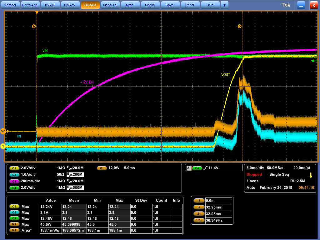
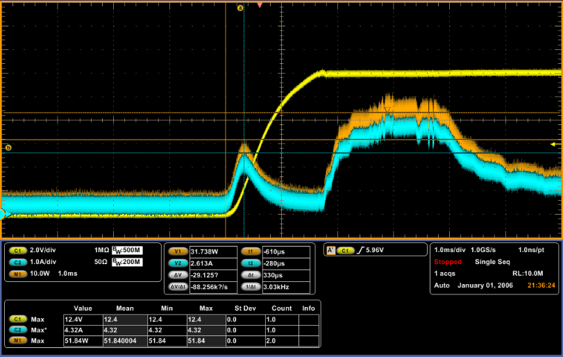
(2) HDD inrush current max IIN is 3.8A, but our design target inrush current is 1A.
Why it has not stay 1A? whether these may damage to the IC internal?
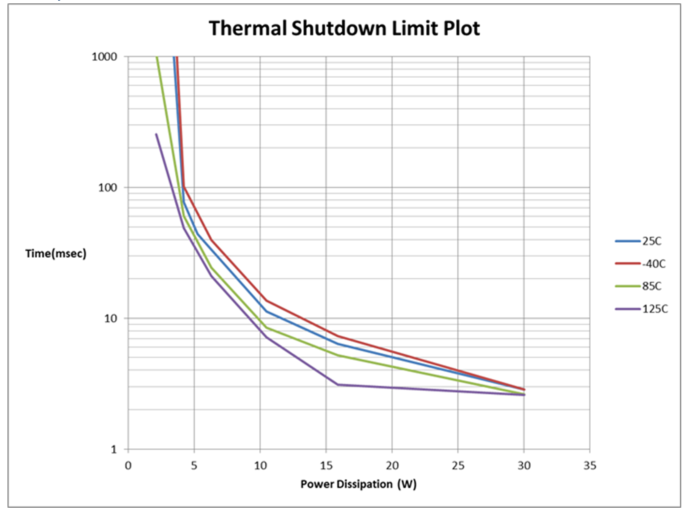
Please help clarify questions and provide SOA information.
Thank you.

(1) Channel1: VOUT, Channel2: IIN, Channel3: Power good, Channel4: VIN

(2)Channel1: VOUT, Channel2: IIN, Channel3: +12V_EN, Channel4: VIN

  • Hi User,

    Welcome to E2E !
    I will look into this and reply by tomorrow. Meanwhile can you please share your project information.

    Best Regards,
    Rakesh
  • 1.End Customer Name: Fujitsu 
    2.Project Name: CX400 M5 
    3.Application: Server 
    4.EAU(Estimated Annual Usage): 10K 
    5.Life Cycle: 2 years 
    6.MP Schedule: Apr. 2019
    7.Target Price: N/A
  • Hi Rakesh,

    Received to reply from FAE Shaquille-Chen at PM 5:00 Taiwai time,
    2. The inrush current max of IIN was 3.8A, but our design target inrush current is 1A.
    Why it has not stay 1A? whether these may damage to the IC internal?
    Please help check SOA and provide information to us.

    FAE's reply :
    Have you selected the right dVdt cap value as per their target inrush current? Here are the equations?
    SR(V/ms)= Iinrush(mA)/Cout(uF)
    Cdvdt(pF)=5300/SR(V/ms)
    For example, if they have a Cout of 470uF and VIN = 12V and need Inrush = 1A, they need to use a CdVdt = 2500pF.

    EE'S reply :
    The setting value for our design as below,
    Output Capacitance : 239.2 uF
    Target inrush current: 1000 mA
    Output Slew Rate dV/dt: 4.180602007 V/ms
    Cdvdt: 1.26776 nF
    So I think our design to use 1.2 nF there is no problem , right?

    The inrush current max of IIN was 3.8A with HDD load per question2,

    whether these may damage to the IC internal and is it compliant with SOA? This is end customers want to know first.

    Why it has not stay 1A? This is is not expected, this is secondary question.

  • Hi User,

    (1) To reduce Vin ringing -> use shorter input cable to minimize input inductance or add decoupling capacitance at the device input.
    Are you using TVS diode at the input.?

    (2) Correct, you need to use 1.2 nF for Cdvdt.

    (3) For eFuses, we don’t publish the SOA curves since the FET reliability is guaranteed using the internal thermal shutdown mechanism.


    Best Regards,
    Rakesh
  • Hi Rakesh,

    (1) To reduce Vin ringing -> use shorter input cable to minimize input inductance or add decoupling capacitance at the device input.
    Are you using TVS diode at the input.? -->Yes, we use a TVS diode VR 15V and VBR 16V on input side.
    (3) For eFuses, we don’t publish the SOA curves since the FET reliability is guaranteed using the internal thermal shutdown mechanism.
    -->So we can judge this inrush current 3.8A is meet SOA.


    .

  • Hi,

    Thanks for the details.

    Regarding SOA: For eFuses, we need to calculate power dissipation (Pd=0.5*Vin*Iinrush current) and then check on power dissipation curve whether the device serves without going into thermal shutdown or not.

    Best Regards,

    Rakesh

  • Hi,

    Use, PG output to enable the downstream load so that the inrush current due to the load can be reduced.

    Best Regards,
    Rakesh
  • Hi Rakesh,

    Why the power dissipation calculation is "0.5*Vin*Iinrush current"?

    We got new result from customer that they are able to push the load current after Vout raise up to 12V by use 10pF dVdt cap.

    The result as below waveform. The math waveform was calculate by (Vi-Vout) * Iin. Is the result within the thermal spec. of TPS25982?

    Thanks

    Shaq

  • Hi Shaq,

    During inrush interval, current will be constant and vout rises linearly so the area under the product equals 0.5*Vin*Iinrush current.

    If the output is fully developed and FET is fully ON, the power dissipation = i(square) * Ron. Since Ron of TPS25982 is 3mohm, the power loss at 4 A load current is 4*4*3mOhm = 48mW.

    Best Regards,
    Rakesh
  • Hi Shaq,

    Please let me know if you still has issues

    Best Regards,
    Rakesh
  • Hi Shaq,

    I am treating this as resolved. Please feel free to post if you still have issues

    Best Regards,
    Rakesh