This thread has been locked.

If you have a related question, please click the "Ask a related question" button in the top right corner. The newly created question will be automatically linked to this question.

UCC27714: Abnormal High-side Waveform

Part Number: UCC27714

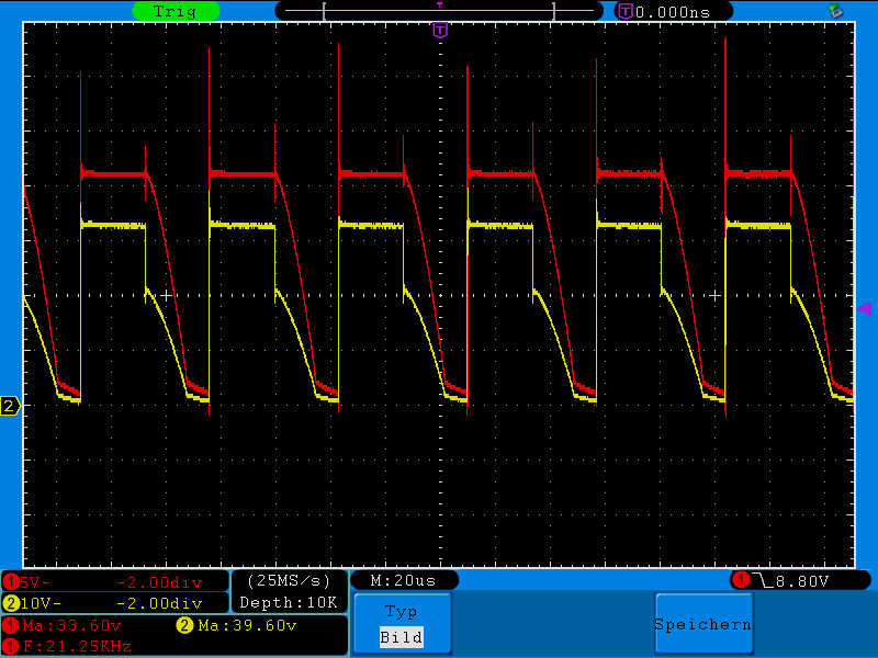
Hi, I'm having problem's with the high-side output of the UCC27714. I connected a Resistor of 900 Ohm between source of the high-side MOSFET and GND. I applied a frequency to the HI-pin via a frequency generator. I scoped the output voltage and and it seems abnormal, because the Voltage just slowly falls to Ground. If i increase the supply voltage to 30V the high side-driver is damaged. I scoped the output voltage and the Gatevoltage on the high-side MOSFET. I think, that the bootstrap cap is not correct discharged...

Please help...

  • Hello Christian,

    Thank you for the interest in the UCC27714. I will work to resolve your concerns in the application.

    First I would confirm the value of C11, bootstrap capacitor, in the UCC27714 datasheet section 9.2 typical application. Since the operating frequency is fairly low, it looks like ~20kHz, also confirm that the gate to source resistance will not discharge the bootstrap capacitor too fast. I would recommend not lower than 20K Ohms, I cannot confirm the value on the schematic.

    The capacitor value is based on the MOSFET gate charge, operating frequency and VDD level. The VDD capacitance should be at least 10x the bootstrap capacitance, which may be OK, but it is hard to read the values on the schematic.

    I assume the yellow trace is the HO output to ground and the red trace is the HS switch node, please confirm. The scope plots are two different voltage scales, it is easier to see the HO to HS voltage if the voltage scale is the same, with the same ground reference location.

    Also confirm the values of the gate driver input filters. It is good practice to have placeholders for the R/C filter on the LI and HI input pins, but the input signals should not have slow rising and falling edges, to avoid multiple triggering due to noise exceeding the threshold hysteresis.

    Confirm the HB capacitor values, and review the gate to source resistance. If you need to post additional questions provide scope plots with HO and HS on the same scale.

    Regards,

    Richard Herring