This thread has been locked.

If you have a related question, please click the "Ask a related question" button in the top right corner. The newly created question will be automatically linked to this question.

TPS62082: Having trouble producing 3.3V with TPS62082DSG

Part Number: TPS62082

Hi, 

We recently started using the fixed 3.3V version of the TPS62082 (TPS62082DSG) switching regulator and are finding that the output is off by about 60 - 50 mV (3.24V instead of expected 3.3V).

We suspect that it's due to our inductor choice having a larger DC resistance, but are not completely sure.

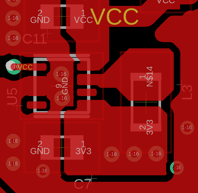
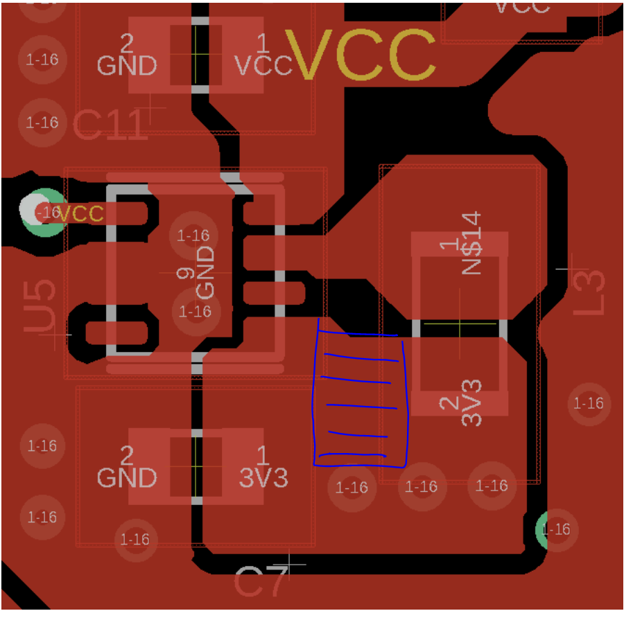
Attached is a snapshot of our circuit and layout and listed below are the PN for the passives:

C11: GRM188R61C106KAALD

L3: DFE201210U-1R0M=P2 (95 mOhms max DC Resistance)

C7: GRM188R60J226MEA0D

Could we receive some assistance in optimizing our output to achieve 3.3V? This is a time sensitive issue and any help would be greatly appreciated. 

  • Hello,
    to better support I need some info:
    1) At which input did you test the board (when you see this drop at the output)? Are you sure to not be in 100% mode?
    2) Where did you measure the Vout? Across Cout or somewhere else?
    If you want you can have a look to the 100% mode on page 10 of the D/S, section 8.3.2.
  • Hi Alfonso,

    Thank you for getting back to me.

    To answer your questions:

    1. We tested the board after providing 5V to the Vin

    2. We tested the output across Cout (C7 in the schematic) and along different points on our design and still measured 3.24V.

    3. How can we tell if we are in 100% mode?  According to the datasheet in section 8.3.2 this mode seems to be enabled when the Vin drops below a certain level. The datasheet doesn't really specify how to enter this mode.  We are providing 5.0V during this test so I don't think it's in 100% mode.

    4. Do you think it has anything to do with our inductor selection? It does have a higher DC resistance than some of the inductor recommended by TI in the datasheet.

    -Josh

  • Hello,
    The formula in section 8.3.2. allows you to evaluate if you are in 100% mode or not. Roughly speaking this happens when Vin is close to Vout, and this is not your case since the input is 5V. Can you tell me which is the voltage at the FB pin during your test?
  • Hi Alfonso,

    The measured voltage at FB (pin 4) is 0V during the test.

    Is this expected?

    -Josh

  • Hello,
    it is expected this value for your application, and it was the first check that I needed to evaluate if the internal feedback was working correctly.
    I need some info about which input and load are used, and especially for the load, I would know the value of the required current. Can you take a scope plot of Vin, Vout, IL (inductor current) and Vsw (switching node)?
  • Hi Alfonso,

    Here is the info you requested.

    Vin: 4.90V (we checked using the oscilloscope and a multimeter and they were the same with no fluctuations)

    Vout: 3.23V (checked using oscilloscope and multimeter and they were the same with no fluctuations)

    IL: We did not measure this yet

    Vsw: (measured at pin 7 SW) - see oscilloscope photo figure 1

    Figure 1 - Vsw

  • Hello,
    The waveform doesn't look good, and it seems that your device is in discontinuous mode. So, can you tell me how and what is connected to the input and output of your device? Which current is required by your load?
  • Hello,
    Do you have any news or the info I requested last time?
  • Hi Alfonso,

    The Vin supplied is usually 5V.

    The load connected to Vout required anywhere from 100 mA to 800 mA but it's normally 100 mA (the measurements I provided were for a load of 100 mA).

    This doesn't seem like a lot.... 

    Would this put the switcher in discontinuous mode?

    According to the datasheet this would happen if the inductor current became discontinuous. I'm worried our inductor selection could be the issue since we went with an inductor with a much higher DC resistance  (I'm just stabbing in the dark here).

    Thank you.

  • Hello,
    With 100mA you can be in discontinuous mode, so can you test the output voltage with an higher output current (let's say at least 500mA or at your maximum 800mA)? Is your input a battery? In theory, the higher DCR should be compensated by the feedback, but if you have an inductor with a lower DCR (similar to the inductor on our EVM), we can remove any doubt with this test.

  • Hi Alfonso,

    Ok, we will conduct the following test:

    1. Induce a load of 500 to 800 mA and measure the Vout from the switcher.

    To answer your question:

    1. We are seeing this 3.24V result with (see schematic snapshot that shows the charger with USB / Battery input):

       - a single cell LiPo connected to a TI charger IC

       - with a 5V USB charger supply

       - with both Battery and USB charging

    The picture below shows the TI charger with Battery and USB (5V) input. The 'OUT' signal from the charger is the Switcher 'Vin'

  • Hello,
    Can you also take a scope plot of the output of this charger (input of TPS62082) to see the ripple (AC coupling on the oscilloscope)? Are also connected other IC to the output of the charger?
  • HI Alfonso,

    We checked the output from the charger earlier and found no ripple. It was a very steady 5V output to the switcher input.

    Yes, the charger 5V output is connected to several other components:

    1. two LEDs

    2. a 2.8V regulator

    Also, we did not do a 500 mA test ( yet ) but we did a 240 mA test and found that the voltage was still 3.24V.

    We are going to provide the 500 mA test results today.

    See pictures

  • Hello,
    what about your test with higher load current? Any possibility to have also the scope plots of the inductor current?
  • Hi Alfonso,

    We tested the switcher with a 770 mA load.

    The results were:

    3.21V - 3.23V from the switcher output

    When we run at 100 mA load we get:

    3.24V - 3.25V

    Does this help to pinpoint the issue?

    Thank you again.

  • Hello,
    can you please measure the output voltage (between pin 5 and 2) again with the oscilloscope and then with a multimeter. Can you also measure the input voltage (oscilloscope and multimeter)? If you have a better oscilloscope (with a higher band) I suggest to use it and can you give me info about the power supply at the input?
  • Hi Alfonso,

    I scoped between pins 2 and 5 on the IC and still get 3.25V.

    The oscilloscope and multimeter readings are the same and there are no fluctuations in the reading on the oscope.

    The voltage input is 4V coming from a TI charger connected to a single cell lipo battery.

    When I use USB power instead the voltage input is 5V.

    In both cases the output from the TPS62092DSG is still 3.25V.

    Attached is a snapshot of the TI charger we are using to power the board from USB or battery.

    The output from the charger 'OUT' is either 5V or 4V depending on the power source.

    This is the Vin for the TPS62082DG.

    Also note:

    - we tried this with several of our boards to see if it was just a bad part.

    - 2 of the switchers output 3.27V - 3.28V and the rest (about 5) output 3.22V - 3.25V, none of the boards output 3.3V

    - In the datasheet of the TPS62082 it says that the output accuracy is +/- 2.5%.

    - Is this possibly why we are seeing 3.25V?

    Thank you for your help Alfonso

  •  Hello,

    I rechecked your layout, trying to understand what is the root cause of your problem. I attach a picture with a suggested cut of the trace close the Vos pin; this is a signal pin that is very sensitive to the noise. Regarding the accuracy is specified only for 0A (load). I am going to close this post, but you can reach me on my email a-furio@ti.com, to support you when you will have the result of this layout's modification.

  • Great, thank you Alfonso. We will try you're suggestion.