This thread has been locked.

If you have a related question, please click the "Ask a related question" button in the top right corner. The newly created question will be automatically linked to this question.

UCC27712: Caps from gate to source

Part Number: UCC27712

Hello,

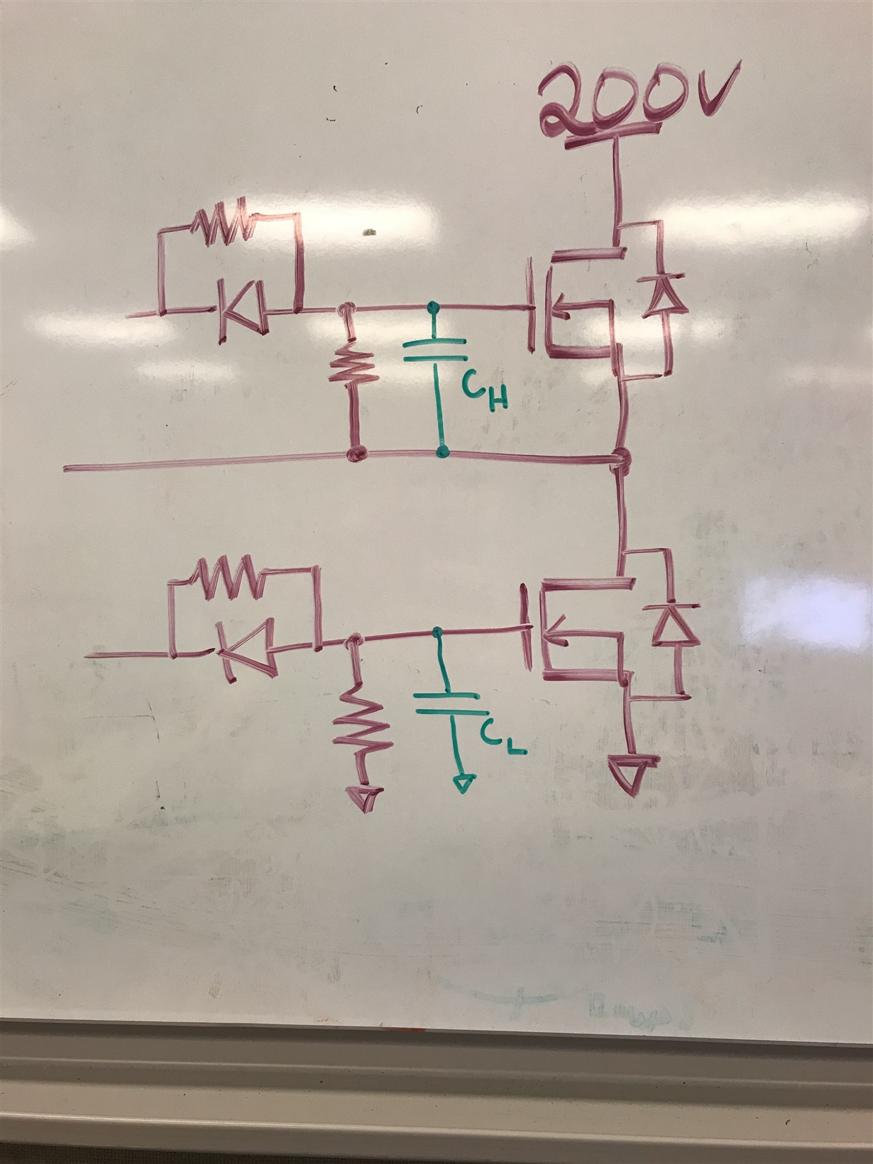
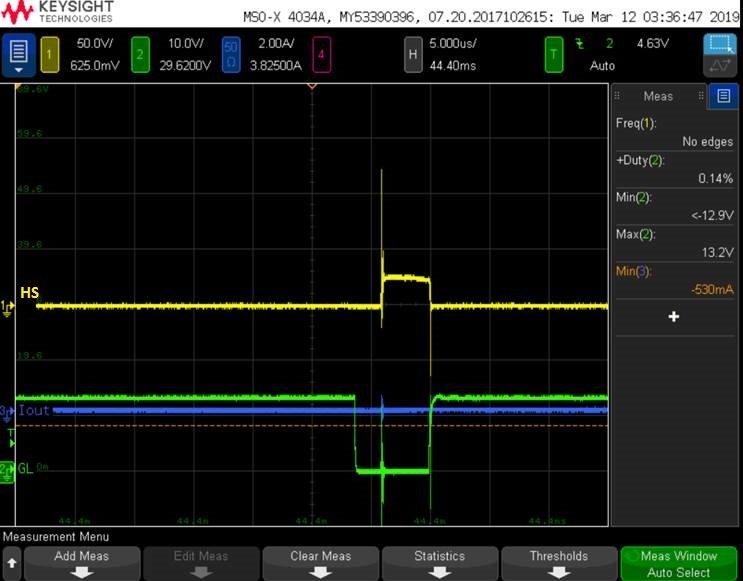
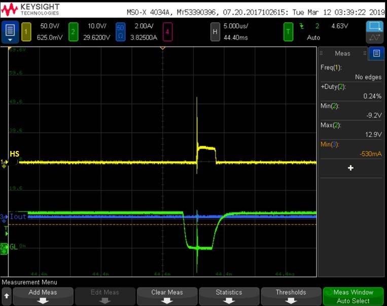
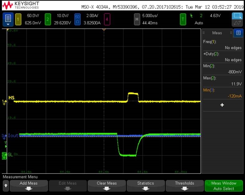
My customer was seeing spikes as shown in Image #1. They were able to remove the negative spike by adding C(L), Image #2, and they were able to remove the positive spike by adding C(H), Image #3.

  1. Is this solution recommended by TI?
  2. We were concerned more with C(H) which feeds back to the boot strap circuit. Any concerns from your end about this?

Note: the images below were collected with supply at 24V, but will need to function at 200V in the real application, C(H)=C(L)=0.1uF/400V.

Circuit


Image #1


Image #2


Image #3


Thank you,
Ryan B. 

  • Hello Ryan,
    Adding capacitance to the MOSFET gate to source is one very valid way to limit the voltage fluctuation on the MOSFET Vgs due to the miller charge injecting current into the gate during the switching transitions. The tradeoffs to confirm are 1) with the capacitance added to the high side MOSFET confirm that the boostrap capacitor value is sized to accommodate the extra charge on Vgs. 2) with the extra charge on the MOSFET Vgs confirm that there is no concern with extra gate drive power dissipation in the gate driver. You can confirm both by referring to the UCC27712 datasheet Section 8.2 typical application.
    If you are happy with the performance, and there are no concerns after reviewing the two recommendations above, there is no reason the additional capacitance on the Vgs is a concern.

    It is likely what you are seeing to some degree, is that the additional capacitance is filtering ringing that will occur from the gate drive loop trace inductance.

    Let us know if this answers your questions, or if you have additional questions you can post on this thread.

    Regards,
    Richard Herring