A related question is a question created from another question. When the related question is created, it will be automatically linked to the original question.
If you have a related question, please click the "Ask a related question" button in the top right corner. The newly created question will be automatically linked to this question.
UCC28064A: Ucc28061 replaced with ucc28064A does not work,
Thank you for your interest in using the UCC28064A. Although it is of the same family of PFC controllers, the -064A is not a direct drop-in replacement for the -061. Many features are the same or similar, but some require different component values to work properly.
I'll need some time to analyze your schematic diagram; but I'll get back to you in a few hours or less with some suggestions to adapt your board to the UCC28064A. Meanwhile, can you please provide your design targets (input range, start-up voltage, output voltage and power level) and the boost inductance that you're using? Thanks,
I am assuming that you simply swapped the UCC28064A into where the UCC28061 was used and made no other changes.
The IC will not work properly, as you have seen. The consequences of this are listed in order of severity:
1. Pin 9 (PWMCNTL) has changed to a burst-threshold function BRST, with a maximum rating of 7V. The 10K resistor RP22 to VCC causes a current stress at the BRST input due to ~7V clamping by an internal ESD protection structure. Fortunately, the current is probably less than 1mA, so the -064A is probably okay. But please remove RP22 for all further operation.
Since you do not have any burst mode with the -061, you can tie pin 9 to GND to avoid burst mode with the -064A.
2. Pin 4 PHB function has changed internally. Now, if PHB is tied to VREF, the -064A will operate only in single-phase mode (Phase-B always turned off.) This will overload Phase-A at > 50% load.
Since you did not use the -061 in 1-phase mode, you can tie pin 4 to GND to keep 2-phase mode always enabled with the -064A.
3. Pin 3 TSET function has changed. In the -061, on-time is proportional to Rtset. In the -064A, on-time is inversely proportional to Rtset.
So to restore the same on-time range, with the -064A Rtset must be reduced to about 24K~27Kohm. The curves of Figure 16 in the UCC28064A datasheet don't have this value, but I estimate it by ratio of ~9us/V Kt for -061 yields a similar 9us/V at low-line VINAC(pk) = 2.5V (assuming 85Vac input) and Kt = ~3.5us/V with Rtset = 66K. 9/3.5 = a factor of 2.5, so Rtset = 66K/2.5 = 25.6K for the -064A at RP30.
4. Pin 7 VINAC has a 7uA hysteresis current in the -061, but this reduced to 2uA in the-064A. To keep the same turn-on and turn-off (Brownout) points, The impedance of the VINAC divider must go up by 7/2. For the -061, you have RP15-18 = 4Meg and RP26 = 91K.
The 4Meg gives you a 28-V hysteresis for Brownout.
To maintain your settings with the -064A, RP15-18 must increase to 14Meg and RP26 = 319K. Choose the closest standard values to these calculations. Filter cap CP13 must reduce from 1000pF to about 300~330pF to keep the same filter time constant. It should be <100us to avoid distortion.
5. Your schematic does not show any by-pass cap on VREF (Pin15). It is recommended to have at least 0.1uF to GND on VREF (see page 31 of the -064A datasheet). The reference regulator stability is compromised without it.
The bypass cap for VCC, CP15, appears to be undersized at 68nF. I recommend at least 1uF or more to handle the peak currents out of the GDA and GDB pins.
With these changes, I hope that your board operates as expected when changing to the UCC28064Acontroller. Note: once changed for the -064A, you can't use the -061 on that board, unless you change them all back again.
thank you very much! We test it according to your method.
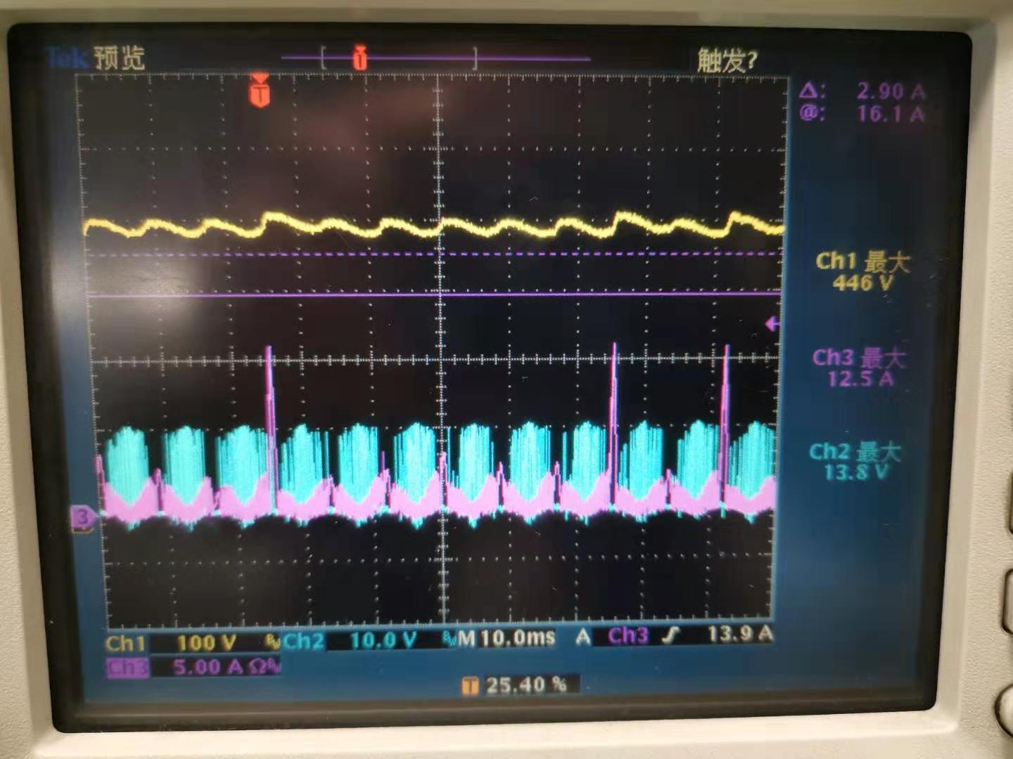
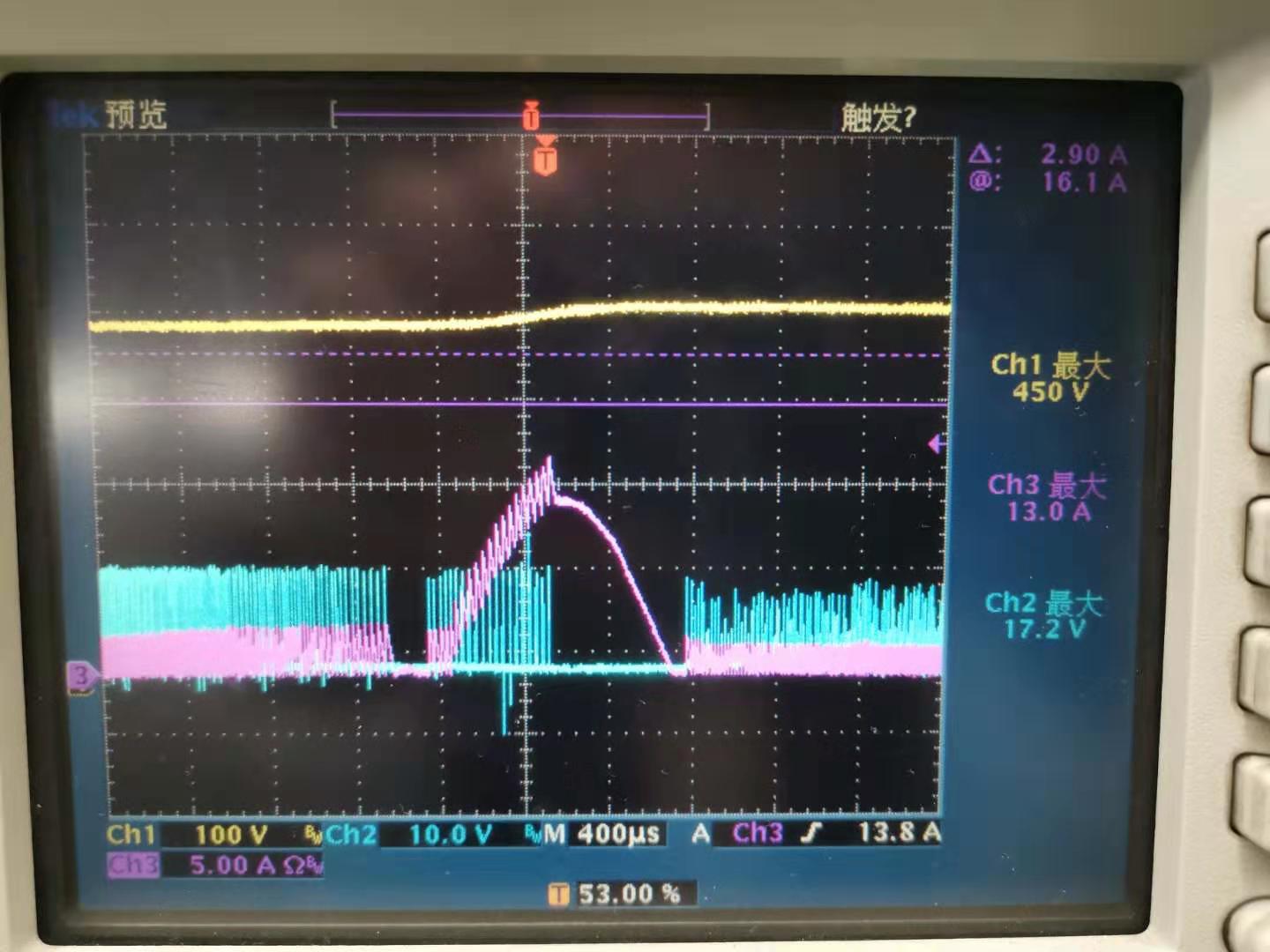
The blue line is the pfc drive. The yellow line is the bus voltage.
Another problem, 28061 current working parameters (input 90 ~ 305v output 425v, 600w, both inductors are 175uh) when input 305V, the input is greater than the output, ucc28061 will work at intervals (305v PFC can not let it work), output The current will have a spike, can you give a suggestion? Is there any optimization for the 28064A? The red line is the inductor current.
I will answer both of your postings in this response.
Most PFC stages, like yours, use the non-isolated-Boost topology to regulate the output voltage.
As you are aware, the output voltage must be higher than the highest peak of the input voltage to avoid a current spike at the peak of the input. For a maximum input voltage of 305Vac, the PFC Vout must be > 431Vdc. In fact, to maintain PFC control it must be several volts higher than the maximum input peak.
In your case, you will always get a peak surge current since there is a direct path from the input to the output through the boost inductor or by-pass diode. The peak of this current is limited only by the difference in voltage (Vin(peak) – Vout – Vdiodes) and the series resistances. The boost MOSFET has no control over this current (regardless of controller, -061 or -064A or any other) and it can be avoided only one way: Vout must be higher than Vin(peak).
The next question is how much higher must Vout be?
Ideally, the PFC controller should control the MOSFET switching over the entire half-line cycle, including the peak. However, it does this only when valid ZCDx signals are detected. If Vout is too close to Vin(peak) the ZCD winding voltage will be too low to meet the threshold criteria at the ZCDx inputs and the controller will stop switching. So there will be some dead spots (no switching) at the peak of the input line. The internal restart timer will attempt to resume switching every ~210us until the ZCD signals are back in spec. The ideal voltage difference will depend on the ZCD winding turns ratio with the boost winding. You must be able to achieve about 2V at ZCDA and ZCDB at the peak of the input line.
So, (Vout –Vin(peak) –Vdiodes))*Nz/Nb > 2V, where Nz/Nb is the turns ratio of the ZCD winding to the boost winding.
There are limit trade-offs to how high the turns ratio should be, because of peak current out of the ZCDx pin during the MOSFET on-time at the peak of the line. Also, choosing a very high turns ratio to minimize Vout will affect performance at the zero-crossings leading to dead-times there (when Vin is too low to trigger the ZCDx thresholds). If your THD specification can tolerate some dead-time at the extreme high-line peak, then a reasonable turns ratio can give you good performance at the zero-crossings.
For the filter on the CS pin, the series resistor should typically be 100R or less, but this is not an absolute requirement. The CS input has an absolute maximum specification of -30mA that it can tolerate. This situation usually happens during the power-up inrush surge when the peak surge current generates a peak negative voltage across the current sense resistor. The CS series resistor limits the current due to this negative voltage to less than -30mA. So if you have a low peak inrush current, you can use a lower series resistance to protect CS. A higher value of Rcs will affect the OCP trip point with an offset voltage due to the bias current (specified at -150uA for -061 and -166uA for -064A) coming out of the CS pin. Once Rcs is chosen, you can adjust the filter capacitor on CS to achieve the degree of noise filtering necessary for your system.
Ideally, no cap should be needed on CS. However, most designs have some amount of switching noise that can couple into the CS input. If this noise is big enough, it will prematurely trigger OCP and shut off PWM until the boost current clears to nearly zero (Vcs < -15mV). This will disrupt normal PFC operation and lead to high distortion of the input curernt. The value of Ccs should be only high enough to filter the noise, not too high, because it forms an RC filter with Rcs and a long time constant can delay OCP response to excess peak currents and allow inductor saturation.
It is best to avoid noise coupling with a good pcb layout, but if your system is particularly noisy and you need high RC filtering on CS, then you can consider to raise the current-sense resistance a bit to compensate for the extra time delay. The final answer is: Yes, you can change the CS-filter R and C values, provided that you are aware of what happens when you do so.